ZEISS Sigma 360 Field Emission Scanning Electron Microscope
| Brand | ZEISS |
|---|---|
| Origin | Germany |
| Model | Sigma 360 |
| Instrument Type | Floor-standing High-Resolution FE-SEM |
| Electron Source | Thermal Field Emission Gun (TFEG) |
| Secondary Electron Resolution | 0.9 nm @ 15 kV, 1.3 nm @ 1 kV |
| Magnification Range | 10× – 1,000,000× |
| Accelerating Voltage | 0.02 – 30 kV |
| Maximum Sample Diameter | ≤ 179 mm |
| Stage | 5-Axis Motorized Eucentric Stage |
| Standard Detectors | In-Lens SE Detector, Everhart-Thornley SE Detector, Solid-State Backscattered Electron (BSE) Detector |
Overview
The ZEISS Sigma 360 is a high-performance field emission scanning electron microscope (FE-SEM) engineered for nanoscale imaging, compositional analysis, and correlative microscopy in academic, industrial, and regulatory laboratory environments. Built upon ZEISS’s proprietary Gemini electron optical column — a dual-lens design integrating precisely balanced electrostatic and magnetic fields — the system delivers exceptional beam stability, sub-nanometer resolution at low accelerating voltages, and minimized specimen charging or deflection, even for magnetic or beam-sensitive materials. Unlike conventional SEMs relying on tungsten or LaB₆ sources, the thermal field emission (TFEG) electron gun provides high brightness, long-term current stability, and excellent energy spread control, enabling consistent signal-to-noise ratios across wide voltage ranges (20 V to 30 kV). The Gemini column’s short working distance capability (as low as 8.5 mm) and 35° take-off angle optimize X-ray collection efficiency for energy-dispersive spectroscopy (EDS), supporting quantitative microanalysis under GLP/GMP-compliant workflows.
Key Features
- Gemini II electron optics with active aberration compensation and ultra-stable TFEG source for reproducible high-resolution imaging down to 0.9 nm at 15 kV and 1.3 nm at 1 kV
- 5-axis motorized eucentric stage with precise tilt, rotation, and XYZ translation — enabling automated multi-region acquisition and tomographic alignment
- Multi-detector architecture: In-lens SE detector for surface topography at low kV; ETSE for high-efficiency secondary electron collection; solid-state BSE detector for atomic number contrast; optional HDBSD for enhanced compositional sensitivity
- Variable Pressure (VP) mode compatibility via C2D or VPSE detectors — permitting imaging of non-conductive, hydrated, or outgassing samples without metal coating
- Integrated aSTEM detector option for scanning transmission electron microscopy (STEM) imaging in SEM configuration, delivering crystallographic and phase contrast at nanoscale resolution
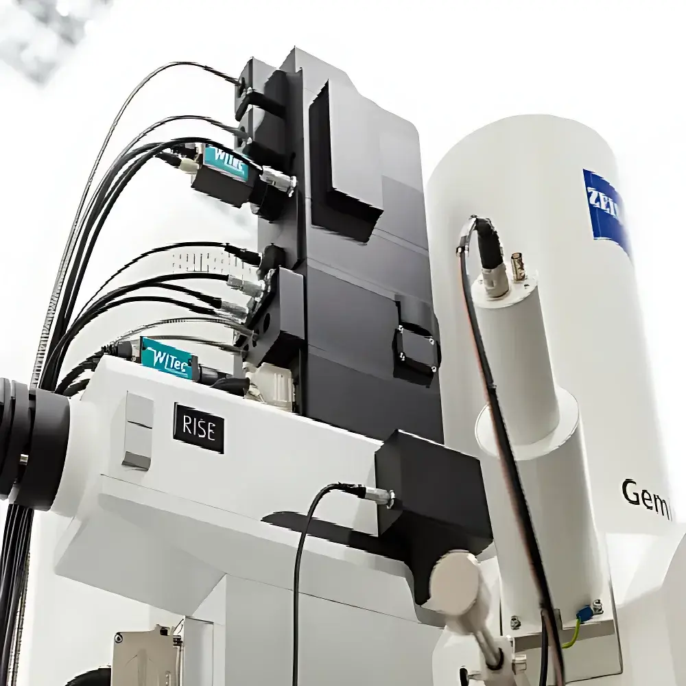
- Modular platform supporting seamless integration of EDS (Sigma Element), EBSD, cathodoluminescence (CL), and Raman spectroscopy (via ZEISS RISE Microscopy)
Sample Compatibility & Compliance
The Sigma 360 accommodates specimens up to 179 mm in diameter and 80 mm in height, compatible with standard SEM stubs, wafer carriers, and custom holders. Its robust vacuum architecture supports both high-vacuum (HV) and variable-pressure (VP) operation — critical for analyzing polymers, biological tissues, ceramics, and geological samples without conductive coating. All analytical modules comply with ISO/IEC 17025 requirements for testing laboratories and support audit-ready data logging per FDA 21 CFR Part 11 when configured with ZEISS SmartSEM software’s electronic signature and audit trail features. The system meets ASTM E1558 (standard guide for SEM image quality evaluation) and ISO 16700 (quantitative EDS microanalysis) specifications for routine QC/QA and R&D applications.
Software & Data Management
Controlled via ZEISS SmartSEM Touch — a role-based, touch-optimized interface — the Sigma 360 enables intuitive operation for both expert microscopists and trained technicians. The software supports parallel SEM and EDS control from a single workstation, eliminating context switching during multimodal acquisition. Advanced scripting (Python API) allows automation of repetitive tasks such as grid mapping, particle analysis, and EDS line scans. All acquired images, spectra, and metadata are stored in vendor-neutral formats (TIFF, .msa, .emi) with embedded calibration and acquisition parameters. Data export complies with MIAME and MIAPE standards for interoperability with third-party analysis platforms including Thermo Fisher Avizo, Oxford AZtec, and Bruker ESPRIT.
Applications
The Sigma 360 serves diverse application domains requiring nanoscale morphological and chemical characterization: semiconductor metrology (line-width measurement, defect review), battery material analysis (cathode/anode particle cracking, SEI layer thickness), additive manufacturing (powder morphology, melt pool porosity), life sciences (cell membrane ultrastructure, nanoparticle internalization), and geosciences (clay mineral identification, pore network quantification). Its low-kV imaging capability ensures minimal sample damage during high-magnification inspection of beam-sensitive organics or 2D materials. When coupled with RISE (Raman Imaging and Scanning Electron) microscopy, it enables spatially registered chemical fingerprinting — correlating functional group distribution (e.g., C=C, Si–O–Si) with nanoscale topography and elemental maps.
FAQ
What vacuum modes does the Sigma 360 support?
The system operates in high vacuum (HV), low vacuum (LV), and variable pressure (VP) modes — selectable via software without hardware reconfiguration.
Is EDS integration fully native or third-party?
ZEISS Sigma Element is a factory-integrated EDS solution with synchronized SEM/EDS acquisition, shared stage control, and unified data handling — not an add-on module.
Can the Sigma 360 perform automated particle analysis?
Yes — SmartSEM includes ParticleMetric software for ISO 13322-1 compliant size, shape, and composition classification of dispersed particles in bulk or on substrates.
Does the system support remote operation and monitoring?
With optional ZEISS Remote Access License, users can monitor live imaging, adjust parameters, and initiate acquisitions from off-site locations via secure TLS-encrypted connection.
What maintenance intervals are recommended for the TFEG source?
Under typical usage (40 h/week), the thermal field emitter requires flash cleaning every 6–12 months and full replacement every 18–24 months — documented in the onboard service log with predictive alerts.


