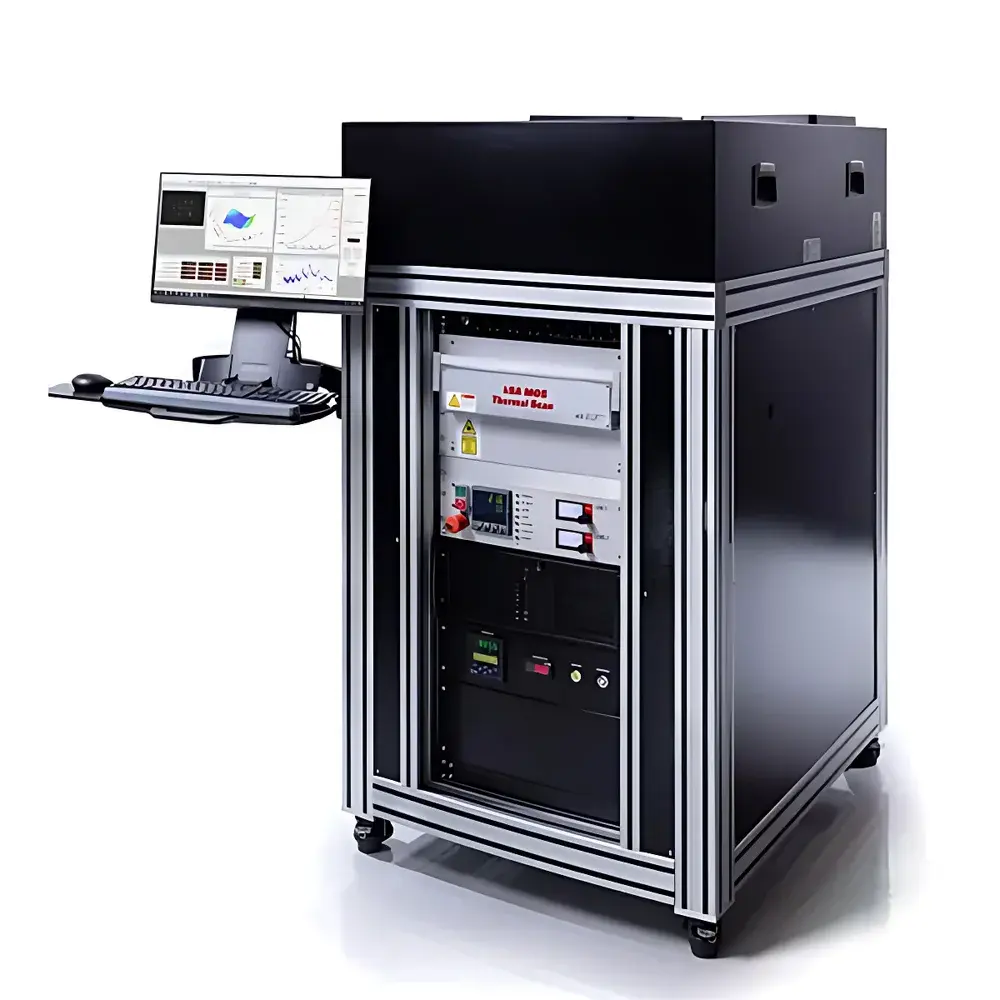
kSA MOS TS Thin Film Thermal Stress Tester
| Brand | k-Space Associates |
|---|---|
| Origin | USA |
| Manufacturer Status | Authorized Distributor |
| Origin Category | Imported |
| Model | kSA MOS TS |
| Price Range | USD 70,000 – 115,000 (approx.) |
| Stress Measurement Range | MPa to GPa |
| Measurement Technology | Multi-Beam Optical Sensor (MOS) Laser Array |
| Operating Temperature Range | RT to 1000°C |
| Curvature Resolution | ≥100 km radius detection limit |
| XY Scan Range | up to 300 mm (optional) |
| XY Scan Speed | up to 20 mm/s |
| XY Step Resolution | 2 µm |
| Compatible Wafer Diameters | 50 mm, 75 mm, 100 mm, 150 mm, 200 mm, 300 mm |
| Temperature Uniformity | ±2°C |
| Environmental Control | Vacuum & low-pressure inert/oxidizing gas (N₂, Ar, O₂) |
Overview
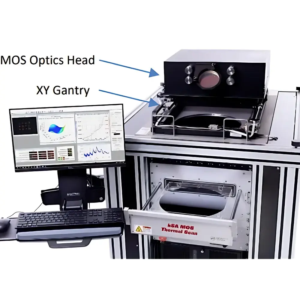
The kSA MOS TS Thin Film Thermal Stress Tester is a high-precision, non-contact metrology system engineered for in-situ and real-time characterization of mechanical stress evolution in thin films during thermal processing. It operates on the Stoney equation principle, deriving film stress from quantitative curvature measurements of substrate bending—enabled by a patented Multi-Beam Optical Sensor (MOS) laser array. Unlike single-point interferometric or wafer-bow profilometric methods, the MOS architecture projects a two-dimensional grid of collimated laser spots onto the sample surface; differential reflection angles across the array are captured simultaneously by a high-resolution CCD detector, enabling sub-microradian curvature sensitivity and spatially resolved stress mapping. Designed specifically for semiconductor process development, MEMS fabrication, and advanced packaging R&D, the system supports dynamic thermal cycling under controlled atmospheres—from ambient air to high-vacuum or reactive gas environments—making it indispensable for studying stress relaxation, interfacial adhesion failure, phase transformation kinetics, and CTE mismatch effects in multilayer stacks.
Key Features
- Non-contact, real-time curvature and stress measurement via MOS multi-beam laser array with simultaneous spatial sampling
- Integrated high-temperature stage with programmable thermal ramping (RT to 1000°C), vacuum-compatible chamber, and gas delivery manifold (N₂, Ar, O₂)
- Closed-loop temperature control ensuring uniformity better than ±2°C across full 300 mm scan area
- Motorized XY scanning platform with 2 µm positional resolution, 20 mm/s max speed, and configurable scan modes: region-of-interest, linear line scans, and full-area raster mapping
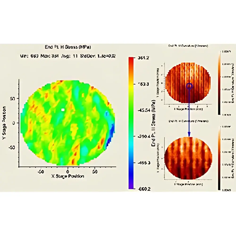
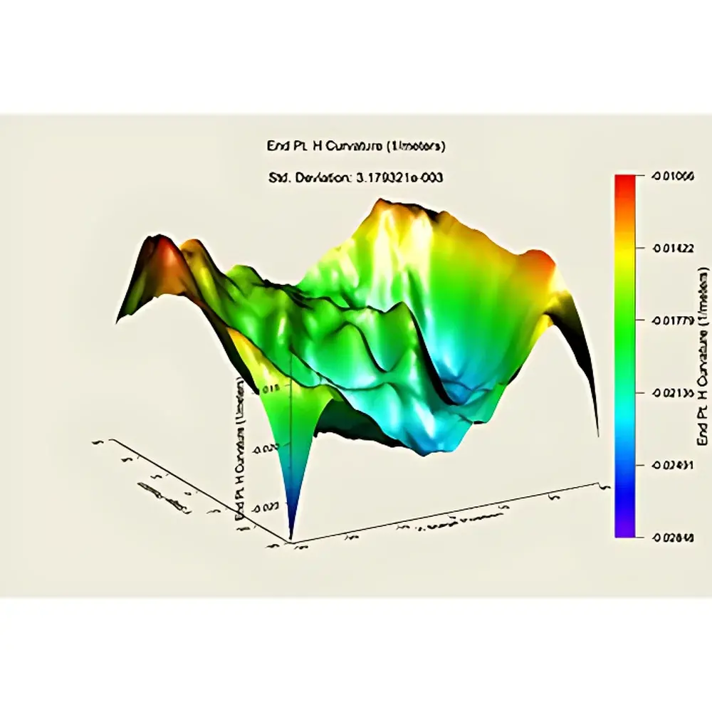
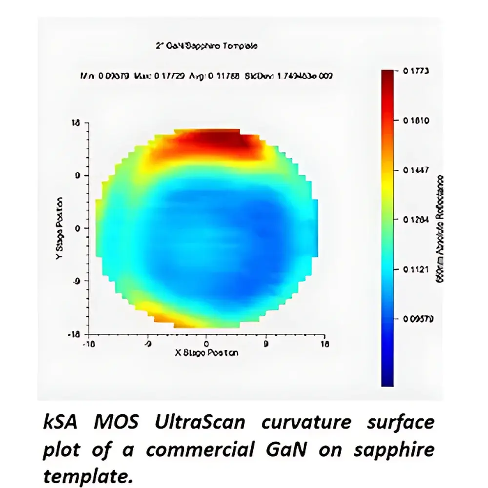
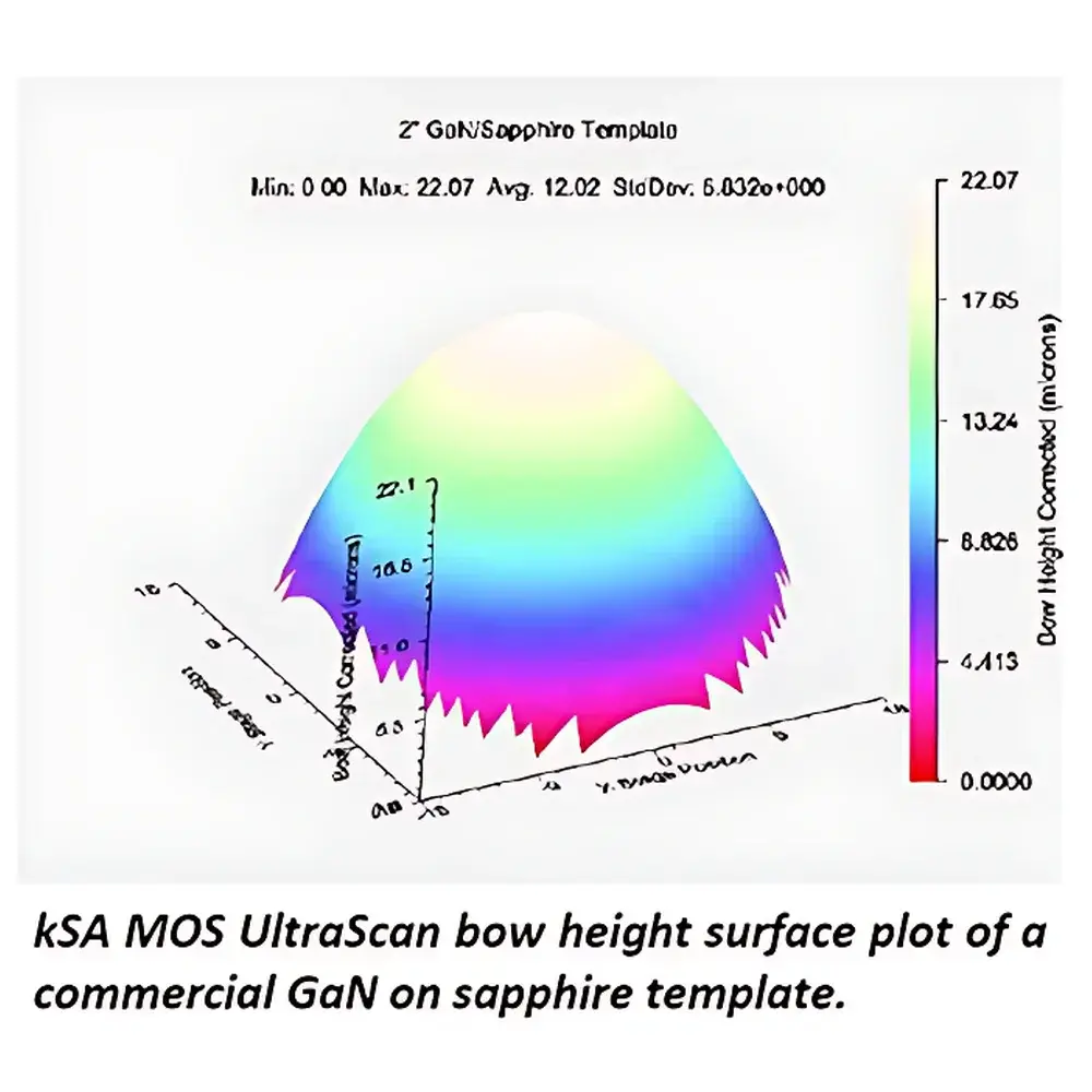
- Quantitative 2D curvature imaging, stress distribution mapping, bow/warp quantification, and 3D topographic reconstruction
- Dual real-time plotting: stress vs. temperature and curvature vs. temperature—synchronized with thermal program execution
- Modular sample holder design accommodating wafers and substrates from 50 mm to 300 mm diameter
- Rapid thermal processing capability: heating rates up to 100°C/min and active cooling options for quenching studies
Sample Compatibility & Compliance
The kSA MOS TS accommodates rigid planar substrates including silicon, sapphire, quartz, glass, SiC, GaN-on-sapphire, and metal foils—provided surface reflectivity exceeds 5% and roughness remains below 5 nm RMS. It complies with ISO 9001 quality management requirements for instrumentation manufacturing and supports audit-ready data integrity workflows aligned with GLP and GMP principles. While not FDA-cleared as a medical device, its measurement traceability is maintained through NIST-traceable calibration protocols for curvature and temperature sensors. The system’s software architecture supports 21 CFR Part 11-compliant electronic signatures, audit trails, and user access controls when deployed in regulated semiconductor fabs or materials qualification labs.
Software & Data Management
Control and analysis are executed via kSA’s proprietary ThermalScan™ software suite, built on a modular LabVIEW-based framework. The interface provides synchronized acquisition of curvature, temperature, gas flow, and stage position data at user-defined sampling intervals (down to 100 ms). All raw sensor outputs—including individual beam angle deviations—are stored in HDF5 format for post-processing reproducibility. Built-in algorithms compute local stress using the modified Stoney equation with substrate thickness, Poisson’s ratio, and Young’s modulus inputs; users may define custom material property libraries per layer stack. Export options include CSV, MATLAB .mat, and TIFF-based stress/curvature maps compatible with ImageJ, Python (NumPy/SciPy), and commercial FEA pre-processors. Batch analysis scripts support statistical reporting across multiple runs—including mean stress, standard deviation, gradient analysis, and defect localization thresholds.
Applications
- Thermal stress profiling of PECVD, ALD, and sputtered dielectric/metal films during anneal cycles
- Residual stress mapping of epitaxial layers (e.g., GaN, AlN) on lattice-mismatched substrates
- Interfacial delamination onset detection via curvature hysteresis analysis during thermal cycling
- CTE mismatch quantification in heterogeneous integration stacks (e.g., Si-to-glass interposers)
- Stress-driven cracking and blistering mechanism studies in low-k porous films
- Process window optimization for rapid thermal processing (RTP) and millisecond annealing
- Qualification of stress-engineered films for MEMS resonators and piezoelectric actuators
- Correlation of in-situ stress evolution with ex-situ XRD, Raman, or TEM structural characterization
FAQ
What physical principle does the kSA MOS TS use to calculate thin-film stress?
It applies the Stoney equation, relating measured substrate curvature to biaxial film stress—using high-resolution differential reflection angles from a 2D laser array to determine local radius of curvature.
Can the system operate under oxidizing or reducing atmospheres?
Yes—integrated mass flow controllers support N₂, Ar, O₂, and forming gas (N₂/H₂); chamber pressure ranges from 10⁻⁶ Torr (UHV) to 1 atm.
Is the software compliant with FDA 21 CFR Part 11 for regulated environments?
Yes—when configured with role-based authentication, electronic signatures, and immutable audit trails enabled.
Does the system require optical access through the substrate?
No—it measures reflection from the film-coated surface; transparent or opaque substrates are equally supported.
How is calibration performed, and what standards are used?
Curvature calibration uses certified radius-of-curvature reference standards traceable to NIST; temperature calibration employs dual-point Pt100 sensor verification against calibrated thermocouples.


