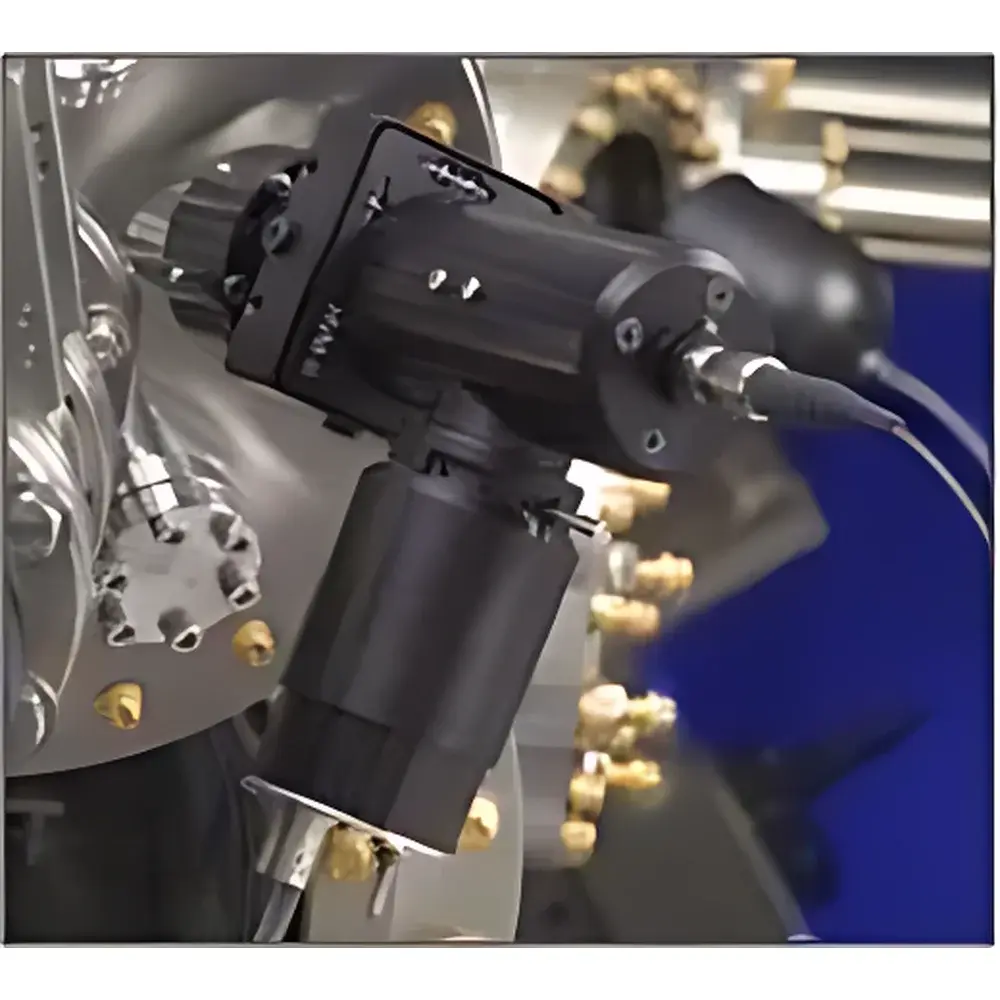
KSA RateRat In-Situ Thin-Film Growth Rate Monitor
| Brand | k-Space |
|---|---|
| Origin | USA |
| Manufacturer Type | Authorized Distributor |
| Origin Category | Imported |
| Model | KSA RateRat |
| Price Range | USD $13,500 – $40,500 (based on configuration) |
| Compatible Target Materials | Metals and Semiconductors |
Overview
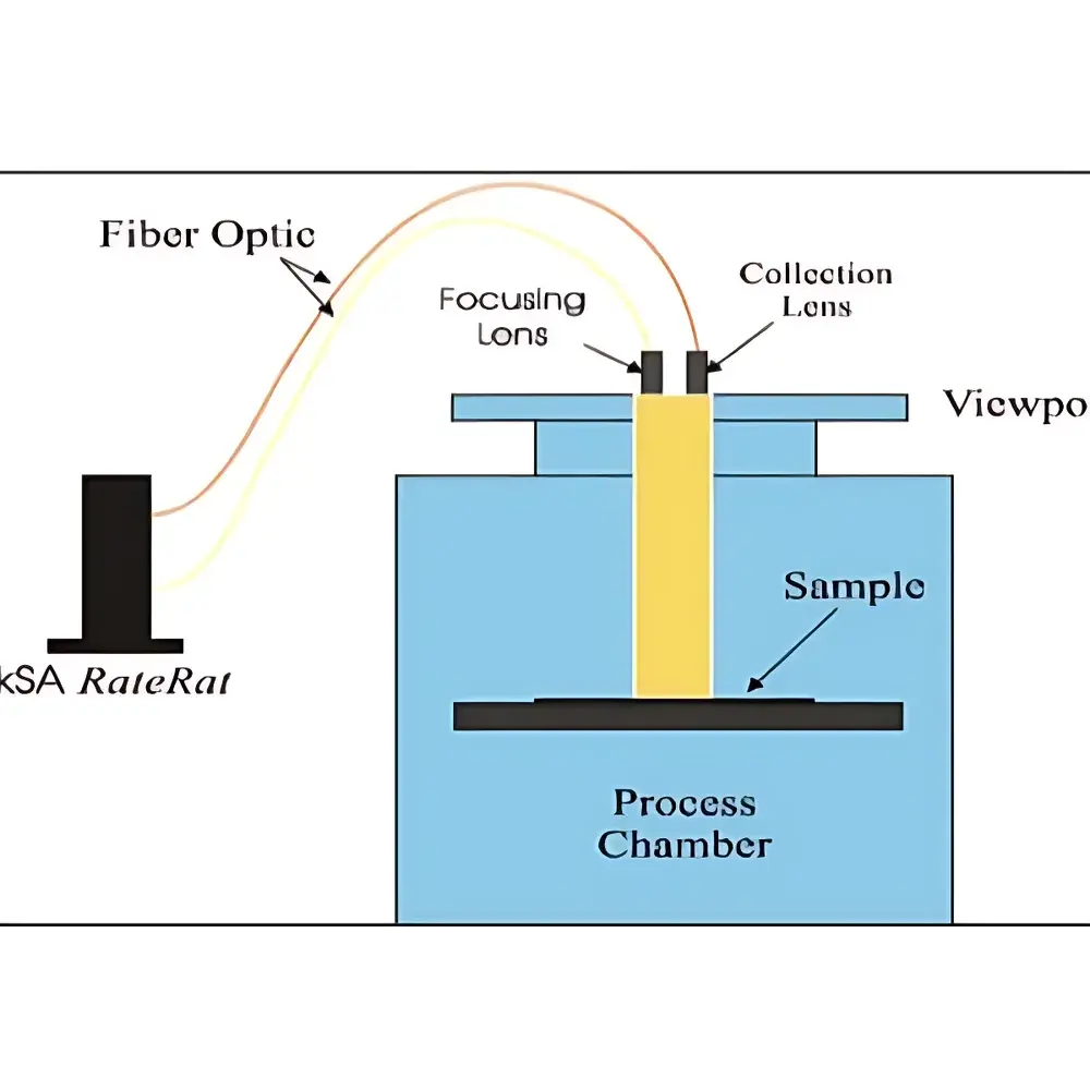
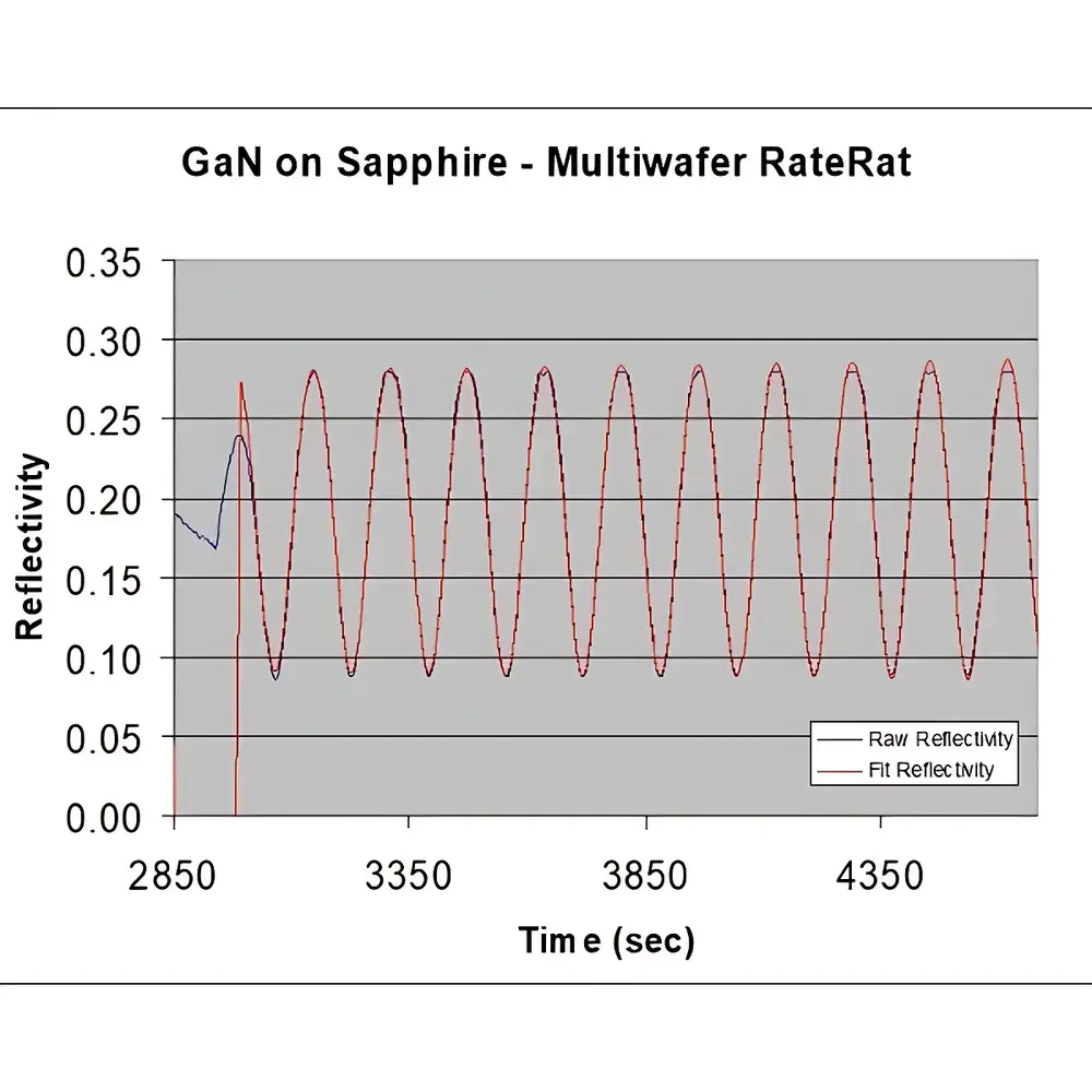
The KSA RateRat In-Situ Thin-Film Growth Rate Monitor is an optical ellipsometry-based metrology system engineered for real-time, non-destructive monitoring of thin-film deposition processes in ultra-high vacuum (UHV) and controlled ambient environments. Utilizing broadband laser reflectance and phase-sensitive interference analysis—principally derived from the principles of variable-angle spectroscopic ellipsometry (VASE) and time-resolved reflectance—RateRat quantifies dynamic changes in film thickness, growth rate (Å/s or nm/s), and complex refractive index (n + ik) during active deposition. It is specifically designed for integration into epitaxial and physical vapor deposition platforms including Molecular Beam Epitaxy (MBE), Metalorganic Chemical Vapor Deposition (MOCVD), DC/RF sputtering, thermal/e-beam evaporation, and pulsed laser deposition (PLD) systems. Unlike ex-situ techniques such as XRR or SEM cross-sectioning, RateRat delivers sub-monolayer temporal resolution with no process interruption, enabling closed-loop feedback control essential for reproducible heterostructure fabrication.
Key Features
- Real-time, in-situ measurement of film thickness (0.1 Å resolution), growth rate (down to 0.01 Å/s), and optical constants (n & k) across spectral ranges typical for UV–VIS–NIR ellipsometric modeling (e.g., 250–850 nm)
- Automated calibration routine using reference substrates and built-in intensity normalization algorithms—no manual alignment required after initial setup
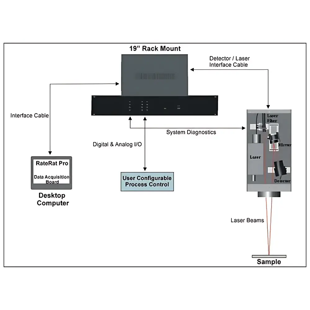
- Integrated feedback interface compatible with standard PLC and process controller protocols (RS-232, Ethernet/IP, Modbus TCP) for real-time actuator triggering (e.g., shutter control, source flux adjustment)
- Multi-layer stack analysis capability: supports sequential modeling of up to 5-layer structures with interfacial roughness and graded composition profiles
- Multi-wafer monitoring mode: synchronizes data acquisition across up to 4 independently positioned sensors for uniformity mapping on 2–6 inch wafers
- Rotating substrate compensation: real-time angular position tracking via encoder input, enabling correction of azimuthal signal modulation during wafer rotation
- Full-parameter acquisition at ≥10 Hz frame rate, with timestamped metadata compliant with ISO/IEC 17025 traceability requirements
Sample Compatibility & Compliance
RateRat supports conductive and dielectric films deposited on crystalline (Si, GaAs, sapphire, SiC), amorphous (glass, quartz), and flexible substrates (polyimide, PET). Compatible target materials include elemental metals (Al, Cu, Ni, Ti), transition metal nitrides (TiN, TaN), oxides (ITO, ZnO, Al₂O₃), III–V and II–VI semiconductors (GaAs, InP, CdTe), and organic small-molecule layers (e.g., Alq₃, NPB). The system complies with CE marking directives (EMC 2014/30/EU, LVD 2014/35/EU), meets UL 61010-1 safety standards for laboratory instrumentation, and supports audit-ready data logging aligned with FDA 21 CFR Part 11 (electronic signatures, audit trails, user access controls) when configured with optional k-Space LabManager™ software.
Software & Data Management
The instrument operates under k-Space’s proprietary RateRat Control Suite—a Windows-based application supporting multi-threaded acquisition, real-time curve fitting using Levenberg–Marquardt optimization, and library-driven optical model generation. All raw interferograms, fitted parameters, and statistical summaries (mean, σ, CV%) are stored in HDF5 format with embedded metadata (timestamp, chamber pressure, substrate temperature, sensor ID). Export options include CSV, MATLAB .mat, and ASTM E1399-compliant XML for LIMS integration. Version-controlled software updates are delivered via secure HTTPS, and firmware revisions maintain backward compatibility with legacy calibration files per ISO/IEC 17025 clause 7.7.
Applications
- MBE growth optimization of quantum well stacks (e.g., InGaAs/GaAs) with layer-by-layer shutter sequencing validation
- MOCVD reactor qualification for GaN-on-Si LED epitaxy, including AlGaN nucleation layer thickness uniformity assessment
- Sputter-deposited TCO (transparent conducting oxide) thickness control in photovoltaic R&D lines
- In-situ monitoring of ALD cycle saturation behavior for HfO₂ and Al₂O₃ gate dielectrics
- Real-time detection of interfacial oxidation or carbon contamination during e-beam evaporation of Au/Ti contacts
- Process window definition for reactive sputtering of TiN under varying N₂ partial pressure
FAQ
What vacuum compatibility does RateRat support?
RateRat’s optical head is rated for UHV operation down to 1×10⁻¹⁰ Torr; feedthroughs meet ConFlat® flange standards (CF-35, CF-63) and include bakeable ceramic insulators.
Can it measure absorbing or opaque films?
Yes—RateRat uses phase-resolved reflectance modeling rather than pure transmission, enabling accurate n/k extraction for metals (e.g., Cr, NiCr) and heavily doped semiconductors where absorption dominates.
Is remote operation supported?
Yes—via k-Space’s LabManager™ Remote Client with TLS 1.2 encrypted session management and role-based access control (RBAC) for multi-user labs.
How is calibration traceability maintained?
Each system ships with NIST-traceable Si/SiO₂ reference wafers; calibration certificates include uncertainty budgets per GUM (JCGM 100:2008) and are archived in the instrument’s internal EEPROM.
Does RateRat require periodic recalibration during long runs?
No—thermal drift compensation is implemented via dual-wavelength referencing and real-time detector gain stabilization; recalibration is only recommended after mechanical shock or optical path contamination.


