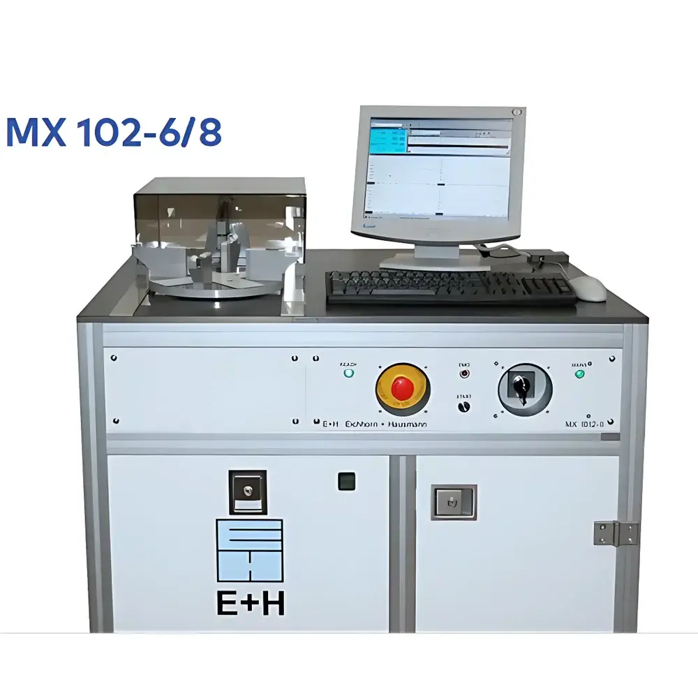
E+H Metrology MX 102-6 / MX 102-8 High-Resolution Wafer Thickness and Total Thickness Variation (TTV) Measurement System
| Brand | E+H Metrology |
|---|---|
| Origin | Germany |
| Model | MX 102-6 / MX 102-8 |
| Wafer Diameter Support | 100 mm, 125 mm, 150 mm, 200 mm |
| Measurement Accuracy | ±0.1 µm |
| Resolution | 10 nm |
| Spatial Resolution | 1 mm |
| Scan Profiles | 4 radial profiles at 45° intervals |
| Software | MX-NT |
| Application | Thickness & TTV metrology post-grinding and post-lapping |
Overview
The E+H Metrology MX 102-6 and MX 102-8 are non-contact, high-precision capacitive metrology systems engineered for rapid, repeatable measurement of silicon wafer thickness and Total Thickness Variation (TTV) in semiconductor front-end process environments. Based on dual-channel differential capacitance sensing, the system measures absolute thickness and surface topography by detecting minute changes in the electric field between two precisely aligned capacitive probes—one positioned above and one below the wafer. This principle enables sub-micron accuracy without physical contact, eliminating risk of surface damage or probe wear during high-throughput inspection. Designed for integration into cleanroom-compatible automation workflows, the MX 102 series delivers full-wafer characterization in under five seconds per sample—making it suitable for both R&D validation and inline process control applications, particularly following mechanical thinning steps such as grinding, lapping, and backgrinding.
Key Features
- Dual-capacitive probe architecture with temperature-stabilized electronics ensures long-term drift stability and metrological traceability to national standards.
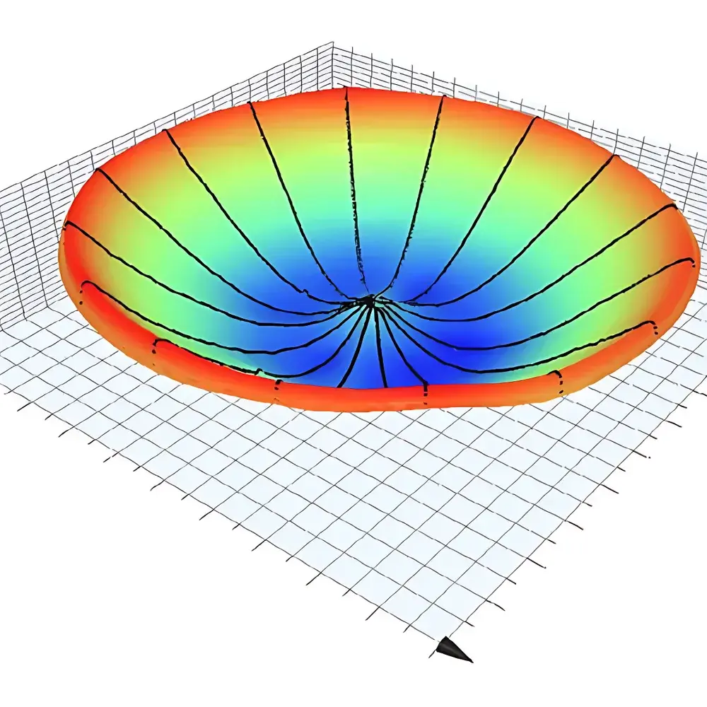
- Four radial scan profiles (spaced at 45° increments) capture >300 localized thickness points per wafer, enabling robust TTV calculation per SEMI MF-1530 and ISO 14407 compliance protocols.
- Configurable spatial resolution of 1 mm allows adaptive sampling density—optimized for either fast screening or high-fidelity defect localization.
- Modular design supports seamless integration with standard SECS/GEM-compliant robotic handlers and FOUP/SMIF load ports via digital I/O and Ethernet/IP interfaces.
- Hermetically sealed sensor heads rated IP54 for operation in Class 100–1000 cleanrooms; compatible with nitrogen-purged enclosures for moisture-sensitive substrates.
Sample Compatibility & Compliance
The MX 102-6 and MX 102-8 support bare and oxide-coated silicon wafers ranging from 100 mm to 200 mm in diameter, including standard thicknesses from 200 µm to 1,000 µm. The system is validated for use with polished, etched, and mechanically processed surfaces—including post-CMP and post-grind wafers exhibiting surface roughness (Ra) down to 0.2 nm. All measurement algorithms adhere to SEMI standards MF-1530 (Wafer Thickness Measurement), MF-1531 (TTV Definition), and ISO 14407 (Geometrical Product Specifications). Calibration procedures follow ISO/IEC 17025 requirements and include documented uncertainty budgets traceable to PTB (Physikalisch-Technische Bundesanstalt) reference artifacts.
Software & Data Management
The MX-NT software platform provides a dedicated metrology interface compliant with industry data integrity frameworks. It features audit-trail logging per FDA 21 CFR Part 11 requirements—including user authentication, electronic signatures, and immutable record retention. Measurement data is exported in standardized formats (CSV, XML, and SECS-II HSMS) for direct ingestion into MES, SPC, and yield management systems. Real-time statistical process monitoring includes X-bar/R charts, capability indices (Cp/Cpk), and automated outlier detection based on user-defined TTV thresholds. Software updates are delivered via secure HTTPS channels with SHA-256 signature verification.
Applications
- Post-grinding and post-lapping thickness uniformity verification in 200 mm and 300 mm wafer fabrication lines.
- R&D evaluation of thinning process parameters—including wheel selection, coolant flow rate, and feed velocity optimization.
- Qualification of temporary bonding/debonding processes where residual stress-induced warpage must be decoupled from thickness variation.
- Support for advanced packaging processes such as TSV (Through-Silicon Via) wafer thinning and fan-out wafer-level packaging (FOWLP).
- Reference-grade metrology for internal calibration labs serving ISO 17025-accredited test facilities.
FAQ
What wafer materials can the MX 102 measure besides silicon?
The system is optimized for conductive or semi-conductive substrates with stable dielectric properties. It has been validated for silicon, SiC, GaAs, and SOI wafers. Non-conductive substrates (e.g., fused silica, sapphire) require custom probe calibration and are supported upon request.
Is the MX-NT software compatible with Windows 11 and 64-bit architectures?
Yes—MX-NT v4.2 and later fully support Windows 10 and Windows 11 (64-bit), with TLS 1.2+ encryption and .NET Framework 6.0 runtime dependencies.
Can the system perform single-side thickness measurement on handled wafers?
No—the dual-probe configuration requires unobstructed access to both front and back surfaces. For handled or bonded wafers, alternative configurations using lift-and-measure stages or vacuum chuck compatibility kits are available.
How often does the system require recalibration?
Under normal cleanroom conditions and daily use, annual calibration is recommended. A built-in self-diagnostic routine verifies probe linearity and thermal drift every startup, with results logged in the audit trail.
Does E+H provide GMP-compliant documentation for pharmaceutical-grade substrate manufacturing?
Yes—upon order, E+H Metrology supplies IQ/OQ documentation packages, URS alignment reports, and 21 CFR Part 11 validation templates for regulated environments including medical device and compound semiconductor production.


