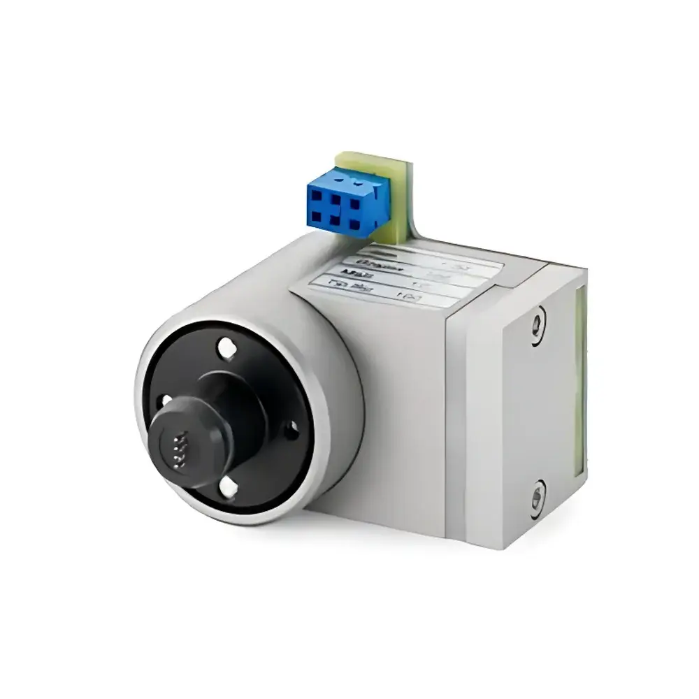
Jandel Cartridge-Type Four-Point Probe Head with 6-Channel Connectivity (CDE-Compatible)
| Brand | Jandel |
|---|---|
| Origin | United Kingdom |
| Model | Cartridge |
| Probe Spacing Options | 0.500 mm, 0.635 mm, 1.00 mm, 1.27 mm, 1.591 mm (±10 µm tolerance) |
| Tip Material | Tungsten Carbide (standard) |
| Tip Diameter | 0.4 mm (standard), 0.3 mm (for high-density spacing) |
| Tip Radius of Curvature | 12.5, 25, 40, 100, 150, 200, 300, or 500 µm |
| Flatness | ≥ ±0.025 mm |
| Tip Load Range | 10 g to 250 g |
| Insulation Resistance | ≥10¹³ Ω at 500 V (between adjacent probes) |
| Probe Arrangement | Linear or rectangular |
| Buffer Zone | 0.5 mm |
| Automation Level | Manual |
Overview
The Jandel Cartridge-Type Four-Point Probe Head is a precision-engineered metrology component designed specifically for integration into CDE (Cambridge Display Engineering) sheet resistance measurement systems. Unlike conventional four-point probe configurations, this cartridge-style probe head features six dedicated electrical connection channels—enabling simultaneous signal routing for dual-probe arrays, reference calibration paths, or auxiliary sensing functions such as contact-force monitoring or temperature compensation. Its operational principle adheres to the classical van der Pauw and linear four-point probe methodologies, where current is injected through two outer probes while voltage is sensed across two inner probes—eliminating contact resistance effects and enabling accurate, non-destructive quantification of surface resistivity (ρₛ) in semiconductor thin films, transparent conductive oxides (TCOs), doped silicon wafers, and emerging 2D materials. The probe’s mechanical architecture is optimized for repeatability under manual operation, with each tungsten carbide tip guided by sapphire bushings to ensure axial stability and minimize lateral deflection during touchdown.
Key Features
- Cartridge-form factor engineered for seamless mechanical and electrical compatibility with CDE-series measurement platforms—including legacy and current-generation CDE 200/400/600 series tools.
- Six independent coaxial connection channels supporting multi-function probing: dual current injection, differential voltage sensing, force feedback, and guard/shield signaling.
- Traceable mechanical certification: Each probe undergoes metrological validation using optical interferometry and high-resolution video profilometry to verify tip radius curvature (12.5–500 µm options), inter-tip spacing (±10 µm tolerance), and planarity (flatness ≥ ±0.025 mm).
- Calibrated tip loading mechanism: Electronic force transducers validate applied normal load across the full 10 g–250 g range; load is transmitted via hardened stainless steel actuators with zero-backlash kinematics.
- High-integrity insulation: Probes maintain ≥10¹³ Ω insulation resistance between adjacent electrodes at 500 V DC—critical for low-leakage measurements on high-resistivity substrates and ultra-thin dielectric layers.
- Modular tip configuration: Standard 0.4 mm diameter tungsten carbide tips; optional 0.3 mm tips available for sub-100 µm pitch applications; osmium–tungsten alloy (50% Os) tips offered for extended wear life on abrasive or textured surfaces.
Sample Compatibility & Compliance
This probe head supports wafer-level characterization of Si, SiC, GaN, InP, and compound semiconductor epitaxial layers, as well as flexible substrates including PET, PI, and glass. It is routinely deployed in Class 100 cleanroom environments and conforms to ISO 14644-1 standards for particulate control when used with appropriate handling protocols. While not an end-user instrument itself, the probe is integral to systems validated per SEMI E10 (Specification for Definition and Measurement of Equipment Reliability, Maintainability, and Availability) and supports process qualification aligned with ASTM F84–22 (Standard Test Method for Measuring Resistivity of Silicon Wafers Using the Four-Point Probe Technique). Its design accommodates standard 100 mm to 300 mm wafer formats and enables edge exclusion down to 2 mm from wafer perimeter.
Software & Data Management
The probe operates in conjunction with CDE’s proprietary acquisition firmware, which implements real-time contact detection, auto-zeroed voltage offset correction, and temperature-compensated resistivity calculation based on user-defined geometric correction factors (e.g., wafer thickness, probe spacing, and sample geometry). All raw analog signals are digitized at ≥18-bit resolution with synchronized timestamping. Audit trails—including probe serial number, calibration date, applied load, and environmental metadata—are embedded into exported .csv and .xlsx datasets. When integrated into GMP/GLP-regulated environments, the host system may be configured to comply with FDA 21 CFR Part 11 requirements via electronic signatures, role-based access control, and immutable data archiving.
Applications
- Process development and monitoring of ion implantation, thermal diffusion, and rapid thermal processing (RTP) steps in CMOS and power device fabrication.
- Uniformity mapping of ITO, AZO, and graphene-based transparent electrodes for display and photovoltaic applications.
- Qualification of ALD and CVD-deposited metal nitride barrier layers (e.g., TiN, TaN) on advanced logic nodes.
- Research-grade sheet resistance profiling of perovskite thin films, MXenes, and other solution-processed functional layers.
- Failure analysis of localized delamination or oxidation-induced resistivity drift in bonded SOI wafers.
FAQ
Is this probe interchangeable with KLA/Tencor or Prometrix four-point probe heads?
No. Although geometrically similar, the mechanical interface, connector pinout, and internal signal routing are proprietary to CDE platforms. Cross-platform use is neither mechanically nor electrically supported.
What verification documentation accompanies each probe?
Each unit ships with a traceable calibration certificate referencing NPL (UK) or NIST-traceable interferometric flatness and spacing measurements, along with force-load verification records and insulation resistance test reports.
Can the probe be used on rough or patterned surfaces?
Yes—provided tip radius and load are selected appropriately. For textured surfaces (e.g., etched Si or polycrystalline films), larger tip radii (≥100 µm) and higher loads (≥100 g) are recommended to ensure stable electrical contact across topographical variation.
How often does the probe require recalibration?
Annual metrological recalibration is recommended; however, in high-throughput production environments, quarterly verification using certified reference wafers (e.g., NIST SRM 2136) is advised to maintain measurement uncertainty within ±2% of nominal value.
Is the black objective turret a functional or cosmetic feature?
It is functional: the anodized black turret serves as an EMI shield and provides precise rotational indexing for multi-spacing probe cartridges—ensuring repeatable alignment without manual re-zeroing between spacing changes.


