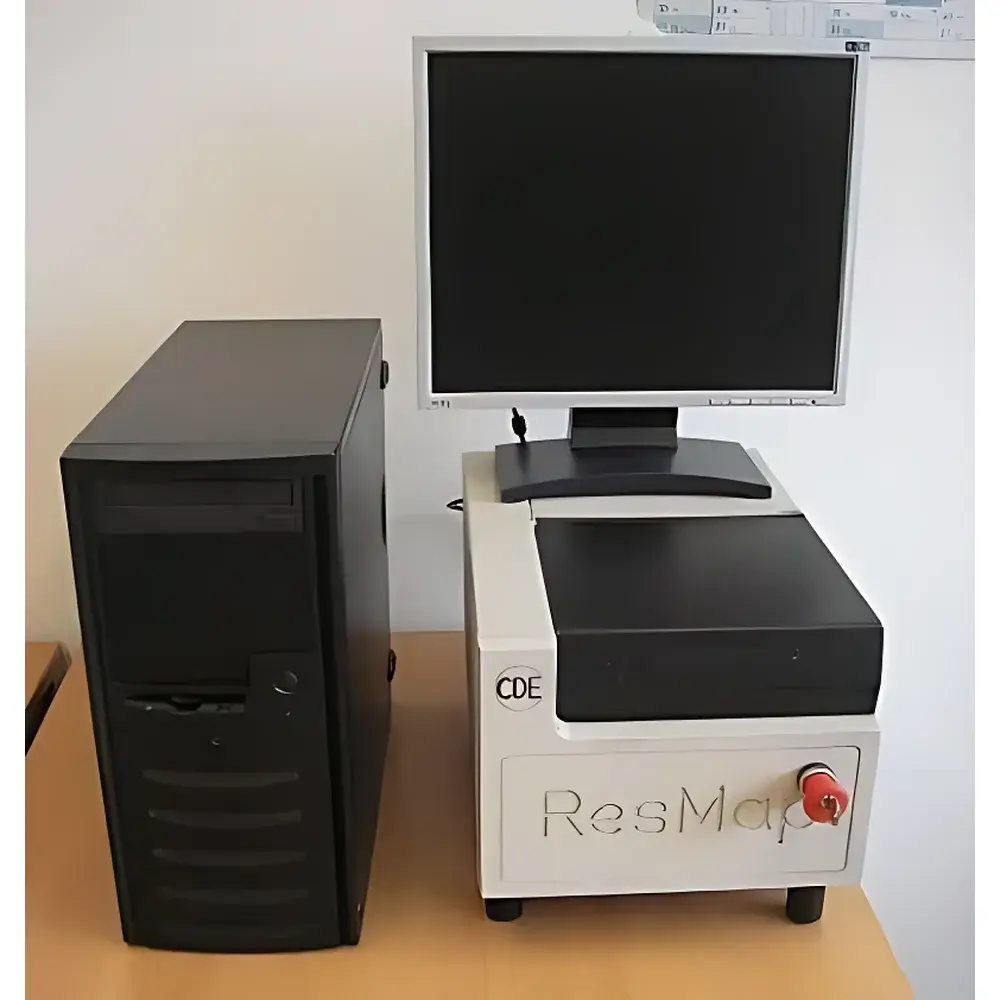

Rayscience CDE ResMap Four-Point Probe Sheet Resistance Mapping System
| Brand | Rayscience |
|---|---|
| Origin | USA |
| Manufacturer Type | Authorized Distributor |
| Product Category | Imported Semiconductor Instrument |
| Model | CDE ResMap |
| Automation Level | Fully Automated |
| Probe Tip Material | Tungsten Carbide |
| Typical Probe Load Force | 100–200 g |
| Compatible Wafer Sizes | 50 mm (2″) to 150 mm (6″) |
| Measurement Mode | Four-Point Collinear Probe (Van der Pauw geometry compatible) |
| Data Acquisition Rate | Up to 4,000 data points per measurement site |
| Interface | Windows-based GUI with recipe-driven operation |
| Calibration Interval | Extended (≥12 months under GLP-compliant usage) |
| Configurable Probe Heads | Dual–quadruple probe head options for 300 mm platform (not included in base model) |
Overview
The Rayscience CDE ResMap Four-Point Probe Sheet Resistance Mapping System is a fully automated, production-grade metrology instrument engineered for high-precision, non-destructive characterization of sheet resistance (Rs) and resistivity (ρ) across semiconductor wafers and photovoltaic substrates. Based on the established four-point collinear probe technique—compliant with ASTM F84 and ISO 10777—the system eliminates voltage drop errors inherent in two-point measurements by separating current injection and voltage sensing functions into distinct probe pairs. This architecture ensures accurate quantification of surface conduction behavior in conductive thin films—including doped silicon, transparent conductive oxides (TCOs), metal layers, and diffusion junctions—without requiring ohmic contact assumptions or geometric correction factors typical of van der Pauw configurations. Designed for integration into cleanroom environments, the ResMap delivers repeatable, traceable, and audit-ready measurements aligned with semiconductor front-end process control requirements.
Key Features
- Fully automated wafer handling and probe positioning with programmable Z-axis force control (100–200 g typical load) ensuring consistent mechanical contact and minimizing film damage or tip wear.
- High-speed mapping capability: up to 4,000 discrete data points per measurement location, enabling statistical process control (SPC) of spatial uniformity across full wafers.
- Collinear tungsten carbide probe tips with calibrated spring-loading mechanism guarantee long-term tip geometry stability and inter-probe spacing accuracy (standard 1.0 mm pitch).
- Windows-based control software featuring recipe-driven operation, real-time contour mapping, and configurable pass/fail thresholds aligned with fab-defined process windows.
- Modular probe head architecture supports dual- or quad-head configurations on 300 mm platforms (optional upgrade), enabling simultaneous multi-site acquisition or cross-directional anisotropy analysis.
- Extended calibration interval (≥12 months) verified against NIST-traceable standards; calibration logs and drift compensation algorithms embedded in firmware.
Sample Compatibility & Compliance
The CDE ResMap accommodates flat, rigid substrates ranging from 50 mm (2″) to 150 mm (6″) diameter wafers, including silicon, GaAs, sapphire, and glass-based photovoltaic substrates coated with epitaxial layers, ion-implanted regions, or deposited metallization. It is validated for use with low-resistivity copper interconnects (down to 1.67 mΩ·cm) and high-sheet-resistance implanted layers (>2 kΩ/□), maintaining measurement linearity across six orders of magnitude (10−3–103 Ω/□). The system meets ISO 9001 quality management requirements and supports GLP/GMP documentation workflows, including electronic signature, audit trail logging (per FDA 21 CFR Part 11), and export of raw data in CSV and XML formats compliant with SEMI E142 standards.
Software & Data Management
The ResMap Control Suite provides a deterministic, deterministic Windows 10/11-native interface with role-based access control, measurement history archiving, and SPC charting (X-bar/R, Cpk). All measurement parameters—including probe sequence, dwell time, current range auto-selection, and environmental compensation settings—are stored as editable recipes. Raw voltage/current pairs are retained alongside derived Rs, ρ, and carrier concentration estimates (via Hall effect correlation models). Data export supports integration with MES systems via OPC UA or custom API endpoints. Firmware updates and diagnostic logs are timestamped and digitally signed to ensure integrity during regulatory audits.
Applications
- Sheet resistance uniformity mapping of diffusion layers, implanted junctions, and annealed dopant profiles in Si, SiC, and GaN wafers.
- Process qualification and monitoring of PVD/CVD metal stacks (Al, Cu, TiN) and transparent electrodes (ITO, AZO) in display and PV manufacturing.
- Correlation of Rs with carrier concentration (n-type/p-type identification) using empirical mobility assumptions and standard calibration curves.
- Thickness estimation of conductive thin films (e.g., NiSi, CoSi2) where resistivity is known and uniform.
- I/V curve acquisition at discrete locations for contact resistance assessment and Schottky barrier height screening.
- Qualification of edge exclusion zones and notch alignment effects in 200 mm and 300 mm wafer handling protocols.
FAQ
What standards does the CDE ResMap comply with for sheet resistance measurement?
ASTM F84 (Standard Test Method for Measuring Resistivity of Silicon Wafers With an In-Line Four-Point Probe), ISO 10777 (Semiconductor devices — Determination of sheet resistance), and SEMI MF1530 (Test Method for Sheet Resistance of Semiconductor Wafers Using a Four-Point Probe).
Can the system measure non-silicon substrates such as GaN-on-SiC or flexible metal foils?
Yes—provided the substrate is mechanically rigid, planar within ±1 µm over the measurement area, and exhibits surface conductivity sufficient for stable current injection (minimum Rs < 105 Ω/□). Flexible or highly curved samples require custom fixturing and are not supported out-of-the-box.
Is the probe head interchangeable between different wafer sizes?
Probe heads are optimized per wafer size family (e.g., 2″–6″ vs. 8″–12″); cross-size compatibility is not supported without mechanical recalibration and firmware reconfiguration—performed only by certified service engineers.
How is traceability maintained for calibration records?
Calibration certificates include NIST-traceable reference standard IDs, uncertainty budgets, environmental conditions at time of verification, and digital signatures. All logs are archived in encrypted internal storage with write-once/read-many (WORM) compliance.


