PL-OE Photoluminescence Imaging System for Solar Cell Production Inspection
| Origin | Hong Kong |
|---|---|
| Manufacturer Type | Distributor |
| Origin Category | Domestic (PRC) |
| Model | PL-OE |
| Pricing | Upon Request |
Overview
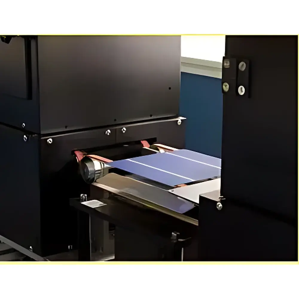
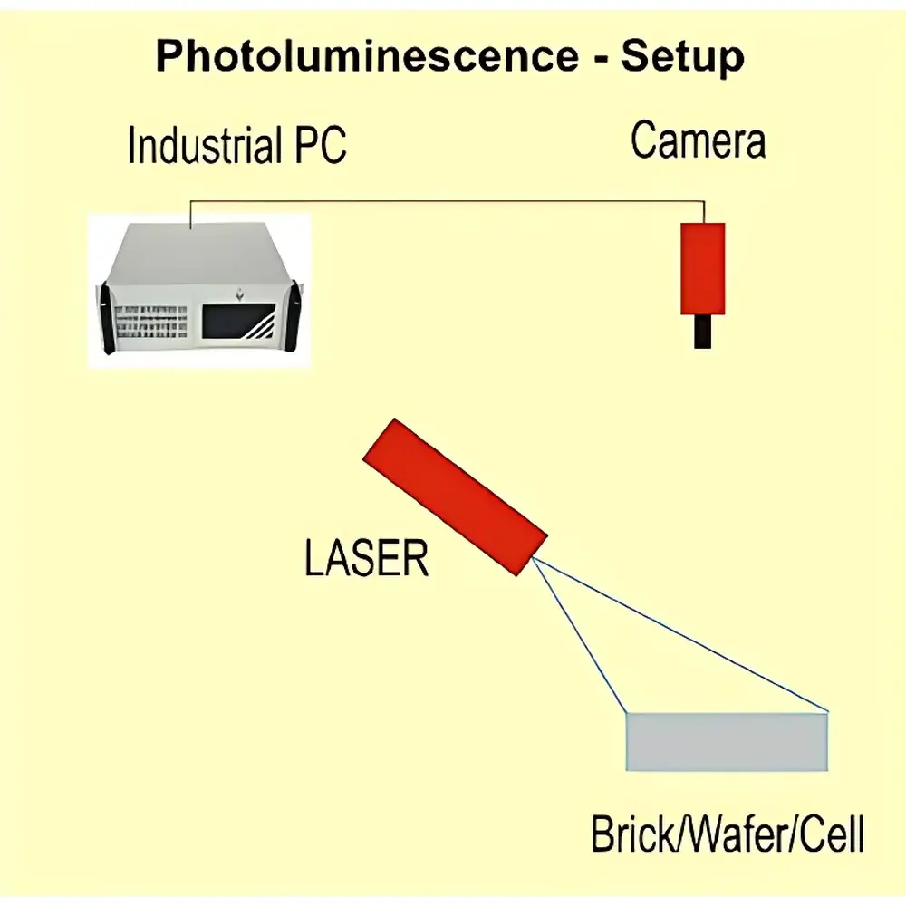
The PL-OE Photoluminescence Imaging System is an industrial-grade optical inspection platform engineered for non-contact, high-throughput defect characterization of silicon photovoltaic (PV) wafers and solar cells during manufacturing. It operates on the physical principle of photoluminescence (PL), leveraging near-infrared (NIR) emission generated under laser excitation to map spatial variations in minority carrier lifetime—directly correlating with material quality, crystal integrity, and junction uniformity. When a pulsed or continuous-wave NIR laser (typically 808 nm or 940 nm) irradiates a silicon sample, electrons are promoted to the conduction band; subsequent radiative recombination emits photons centered at ~1150 nm. Regions with structural defects—such as microcracks, grain boundaries, metal impurity clusters, or shunting paths—act as non-radiative recombination centers, suppressing PL intensity. This contrast mechanism enables quantitative, two-dimensional visualization of subsurface and bulk defects without physical contact or sample preparation.
Key Features
- Industrial-grade cooled deep-depletion CCD imaging sensor (1024 × 1024 pixels, 13 µm pixel pitch, 16-bit dynamic range) optimized for high signal-to-noise ratio (SNR) in the 1000–1300 nm spectral window
- NIR-optimized C-mount lens assembly with integrated long-pass and bandpass filters to suppress laser scatter and ambient IR noise
- Modular laser excitation subsystem compatible with 808 nm and 940 nm diode lasers, configurable for uniform illumination across 6-inch (156 mm) wafers (5-inch option available upon specification)
- Stop-and-go motion control architecture enabling precise synchronization between laser pulse timing, camera exposure, and conveyor-based sample positioning
- Ruggedized enclosure with ESD-safe design and IP52-rated environmental protection for integration into cleanroom-adjacent production lines
- Real-time image acquisition at 2.25 fps full-frame rate, supporting throughput of up to 3000 cells per hour under standard inspection cycle configuration
Sample Compatibility & Compliance
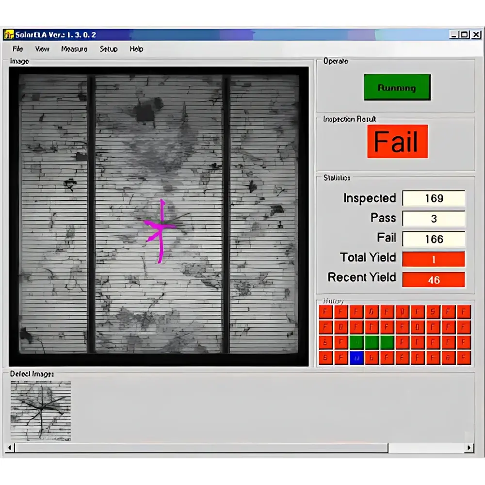
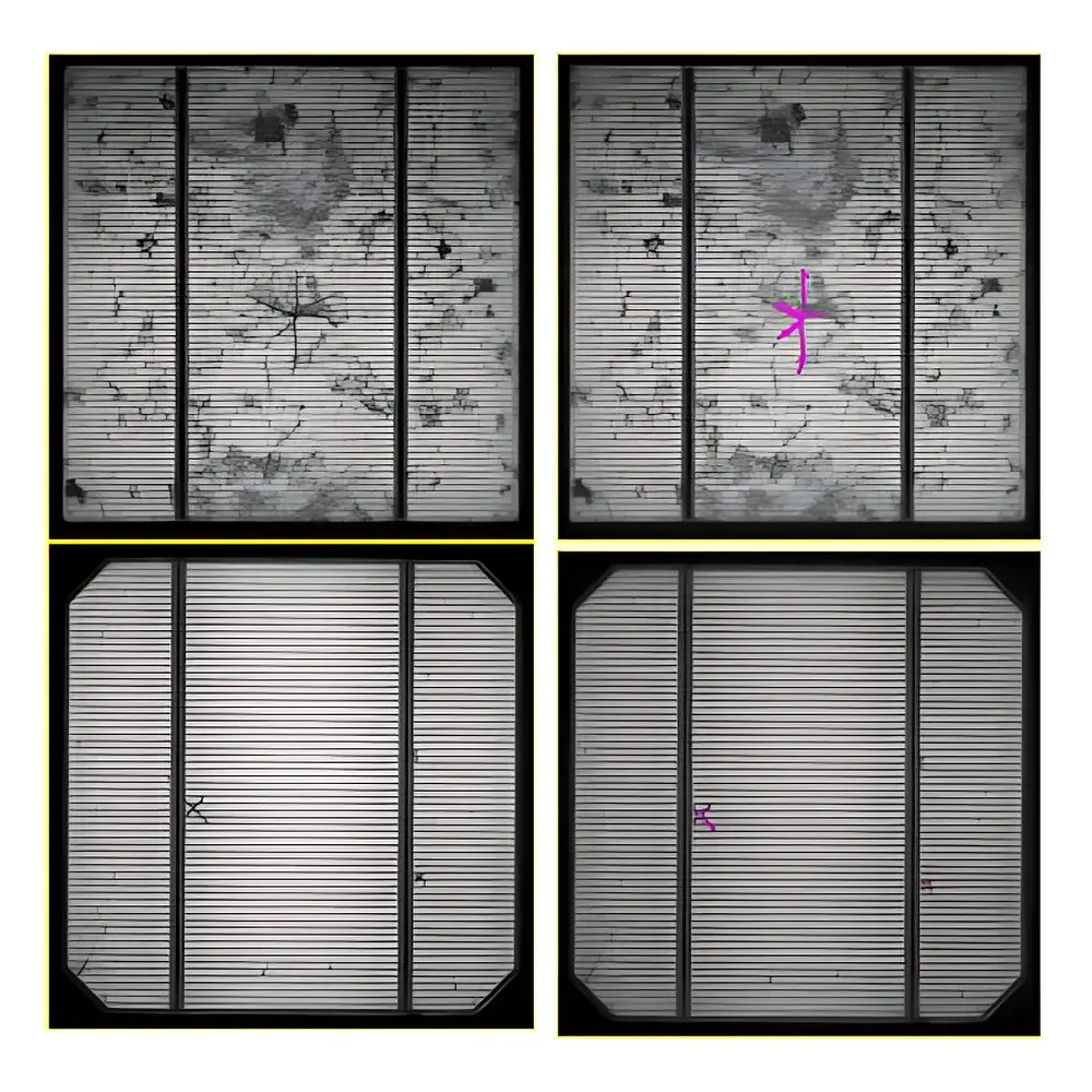
The PL-OE system accommodates standard crystalline silicon solar cell formats including monocrystalline and multicrystalline wafers (6” / 156 mm, with optional 5” / 125 mm configuration), supporting both front-contact (2- and 3-busbar) and back-contact (BC) architectures. It detects critical process-induced defects: microcracks (<5 µm width), macrocracks, dark current regions, low-lifetime zones, edge chipping, and whole-cell shunts. The system meets foundational requirements for ISO 9001-compliant PV manufacturing environments and supports traceability workflows aligned with IEC 61215-2 (MQT 07 – Visual Inspection) and IEC 62788-1 (Material Characterization). While not certified to GLP/GMP standards by default, its hardware architecture and metadata logging structure permit validation for regulated QC applications when deployed with documented SOPs and periodic calibration protocols.
Software & Data Management
The proprietary PL-Insight™ software suite provides calibrated intensity mapping, region-of-interest (ROI) analysis, defect classification templates, and batch-level statistical reporting (e.g., defect density per cm², mean PL intensity, coefficient of variation). All images are stored with embedded EXIF metadata—including timestamp, laser power, exposure time, stage position, and sensor temperature—to ensure audit readiness. Export formats include TIFF (16-bit), CSV (intensity profiles), and PDF reports compliant with internal QA documentation standards. The software architecture supports integration with MES/SCADA systems via TCP/IP or OPC UA interfaces; raw image data can be archived in vendor-agnostic HDF5 format for third-party lifetime modeling (e.g., τeff extraction using calibrated PL quantum yield models).
Applications
- In-line wafer sorting prior to texturing and diffusion—identifying pre-process cracks and contamination-induced lifetime degradation
- Post-metallization inspection to detect firing-induced microcracks and Al-BSF delamination
- Quality gate screening before lamination—rejecting cells with latent shunts or edge recombination hotspots
- R&D correlation studies linking PL contrast patterns with LBIC, EL, and μ-PCD measurements
- Supplier qualification audits—quantifying incoming Si wafer bulk lifetime homogeneity and dislocation density distribution
FAQ
What is the minimum detectable crack width under standard operating conditions?
Typical resolution limit is ~0.15 mm/pixel; sub-pixel cracks may be inferred from intensity gradient anomalies, but definitive detection requires ≥2-pixel width for statistical confidence.
Can the system distinguish between surface contamination and bulk crystal defects?
Yes—through controlled excitation depth modulation (via laser wavelength selection) and comparative analysis with electroluminescence (EL) maps, enabling differentiation between surface recombination (e.g., oxide pinholes) and bulk defects (e.g., dislocation clusters).
Is the PL-OE system compatible with automated handling systems?
Yes—it features standard pneumatic I/O signals (24 V DC), encoder input support, and Modbus RTU communication for seamless integration with robotic end-effectors and conveyor controllers.
Does the system require periodic recalibration?
Annual intensity calibration using NIST-traceable NIR reference tiles is recommended; laser power and sensor gain stability are monitored continuously via built-in photodiode feedback and dark-frame subtraction routines.
What training and documentation are provided with the system?
Includes operator manual, maintenance guide, factory-verified performance test report, and 2-day on-site installation & basic operation training; advanced application workshops available separately.


