SHNTI TEM-SN Silicon Nitride Membrane Windows for Transmission Electron Microscopy
| Brand | SHNTI (Shanghai NTI Instruments) |
|---|---|
| Origin | USA |
| Manufacturer Type | Authorized Distributor |
| Product Origin | Imported |
| Model | TEM-SN |
| Accelerating Voltage Compatibility | Up to 300 kV (compatible with standard TEMs operating at 70–300 kV) |
| Magnification Range | Optimized for high-resolution imaging ≥100× |
| Frame Dimensions | 3 mm × 3 mm |
| Window Aperture | 0.5 mm or 1.0 mm (square) |
| Si₃N₄ Membrane Thickness | 50 nm or 100 nm (customizable from 30–200 nm, MOQ 100 pcs) |
| Frame Thickness | 200 µm or 381 µm |
| Surface Roughness | 0.6–2 nm RMS |
| Thermal Stability | Stable up to 1000 °C in inert/vacuum environments |
| Chemical Resistance | Inert to most acids, bases, and organic solvents (except hot phosphoric acid and strong alkalis) |
| Hydrophobicity | Native hydrophobic surface |
| Cleaning Method | Compatible with O₂ plasma, Ar/O₂ glow discharge, and chemical etching (e.g., Piranha: H₂SO₄:H₂O₂ = 1:1 |
| RCA1 | H₂O:HCl:H₂O₂ = 5:3:3) |
Overview
SHNTI TEM-SN Silicon Nitride Membrane Windows are ultra-thin, low-stress (0–250 MPa) freestanding Si₃N₄ membranes fabricated via advanced MEMS processes on single-crystal silicon frames. Designed specifically for transmission electron microscopy (TEM), these windows serve as robust, atomically flat, and chemically inert substrates for high-fidelity electron-transparent sample support. Unlike carbon-coated copper grids, Si₃N₄ membranes provide a crystalline-amorphous background free of diffraction artifacts, enabling unambiguous interpretation of lattice fringes, strain mapping, and quantitative EELS/EDS analysis. The 50 nm and 100 nm membrane thicknesses ensure optimal electron transparency across the full operational voltage range of modern TEMs (70–300 kV), while maintaining mechanical integrity under high-vacuum conditions and beam exposure. Their nanoscale surface roughness (0.6–2 nm RMS) meets stringent requirements for atomic-resolution imaging and in situ TEM experiments involving catalysis, solid-state reactions, or nanomaterial growth.
Key Features
- Freestanding low-stress silicon nitride (Si₃N₄) membranes with precisely controlled thickness (50 nm or 100 nm standard; custom 30–200 nm available)
- 3 mm × 3 mm silicon frame with polished edges and standardized thickness options (200 µm or 381 µm) for compatibility with standard TEM holders and autoloader systems
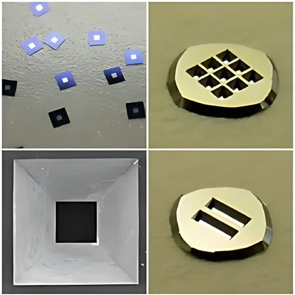
- Aperture options: 0.5 mm or 1.0 mm square windows—optimized for large-tilt TEM tomography and dual-axis acquisition
- High thermal stability: maintains structural integrity up to 1000 °C in vacuum or inert gas, enabling in situ CVD, annealing, and reaction studies
- Chemically inert substrate compatible with aggressive precursors (e.g., TiCl₄, NH₃, silanes) and post-deposition etchants
- No intrinsic carbon contamination—eliminates background interference in EELS, EFTEM, and low-kV imaging
- Plasma-treatable surface: O₂ or Ar/O₂ glow discharge yields reproducible, transient hydrophilicity for uniform dispersion of aqueous colloids and biological specimens
Sample Compatibility & Compliance
SHNTI TEM-SN windows support diverse sample classes including hydrated biomolecules, metal–organic frameworks (MOFs), quantum dots, graphene oxide dispersions, aerogels, and catalytic nanoparticles. Their nitrogen-free composition avoids spectral overlap in N-K edge EELS and prevents false-positive nitrogen signals in EDX quantification—critical for nitrogen-sensitive studies (e.g., nitride semiconductors, nitrogen-doped carbons). The windows comply with ISO 9001 manufacturing protocols and are supplied in Class 100 cleanroom-packaged blister trays. While not certified to GLP or GMP standards per se, their batch traceability, documented surface roughness, and consistent stoichiometry support regulatory-compliant workflows in materials R&D labs adhering to ASTM E2931 (Standard Guide for TEM Sample Preparation) and ISO/IEC 17025–aligned quality management systems.
Software & Data Management
These physical substrates do not incorporate embedded electronics or firmware. However, SHNTI provides full technical documentation—including dimensional drawings (DWG/PDF), thickness certification reports (ellipsometry cross-verified), and cleaning protocol guidelines—to integrate seamlessly into LIMS and ELN platforms. Batch-specific lot numbers enable traceability for audit trails in FDA 21 CFR Part 11–compliant environments where raw material qualification is required. Users may log window usage, plasma treatment parameters, and associated imaging sessions directly within DigitalMicrograph®, SerialEM, or Velox software via custom metadata fields.
Applications
- In situ TEM studies of nanowire growth, phase transformation, and electrochemical cycling using heating, biasing, or gas environmental cells
- Cross-correlative microscopy: precise region-of-interest (ROI) matching between TEM, SEM, AFM, and XPS on identical sample locations
- High-angle annular dark-field (HAADF) STEM of beam-sensitive organic–inorganic hybrids and soft matter
- Low-dose cryo-TEM of vitrified biological specimens—enhanced contrast due to zero-carbon background
- Direct deposition of functional thin films (e.g., MoS₂, perovskites) via CVD or ALD without grid interference
- Support for focused ion beam (FIB)-prepared lamellae when used with multi-pore variants (available upon request)
- Quantitative EDS mapping of light elements (B, C, N, O) without matrix-induced absorption artifacts
FAQ
Can TEM-SN windows be reused after plasma cleaning?
No. SHNTI explicitly recommends single-use operation. Repeated plasma exposure degrades membrane tensile strength and increases risk of catastrophic rupture during TEM vacuum pump-down or beam irradiation.
Why is ultrasonic cleaning prohibited?
Cavitation forces exceed the fracture toughness of sub-100 nm Si₃N₄ membranes. Even brief sonication induces microcracks undetectable by optical inspection but fatal under electron beam stress.
Are custom aperture geometries (e.g., circular, slits, arrays) available?
Yes. SHNTI offers multi-window arrays (3×3, 5×5), linear slit configurations, and patterned pores (≥200 nm diameter) for specialized applications such as electron holography or differential phase contrast (DPC) imaging. Minimum order: 100 pieces.
How does native hydrophobicity affect biological sample loading?
Hydrophobic surfaces cause aqueous droplets to bead, leading to non-uniform particle distribution. Plasma treatment renders the surface hydrophilic for ~2–4 hours—sufficient for grid blotting and vitrification. For extended experiments, in situ plasma activation inside the TEM holder is advised.
Is there nitrogen signal interference in EELS analysis?
The Si₃N₄ membrane itself contributes a detectable N-K edge. However, its spatially fixed, homogeneous intensity allows robust background subtraction using power-law or spline models—standard practice in Gatan Microscopy Suite and HyperSpy. For nitrogen-free background, users may select alternative SiO₂ membranes (offered separately).


