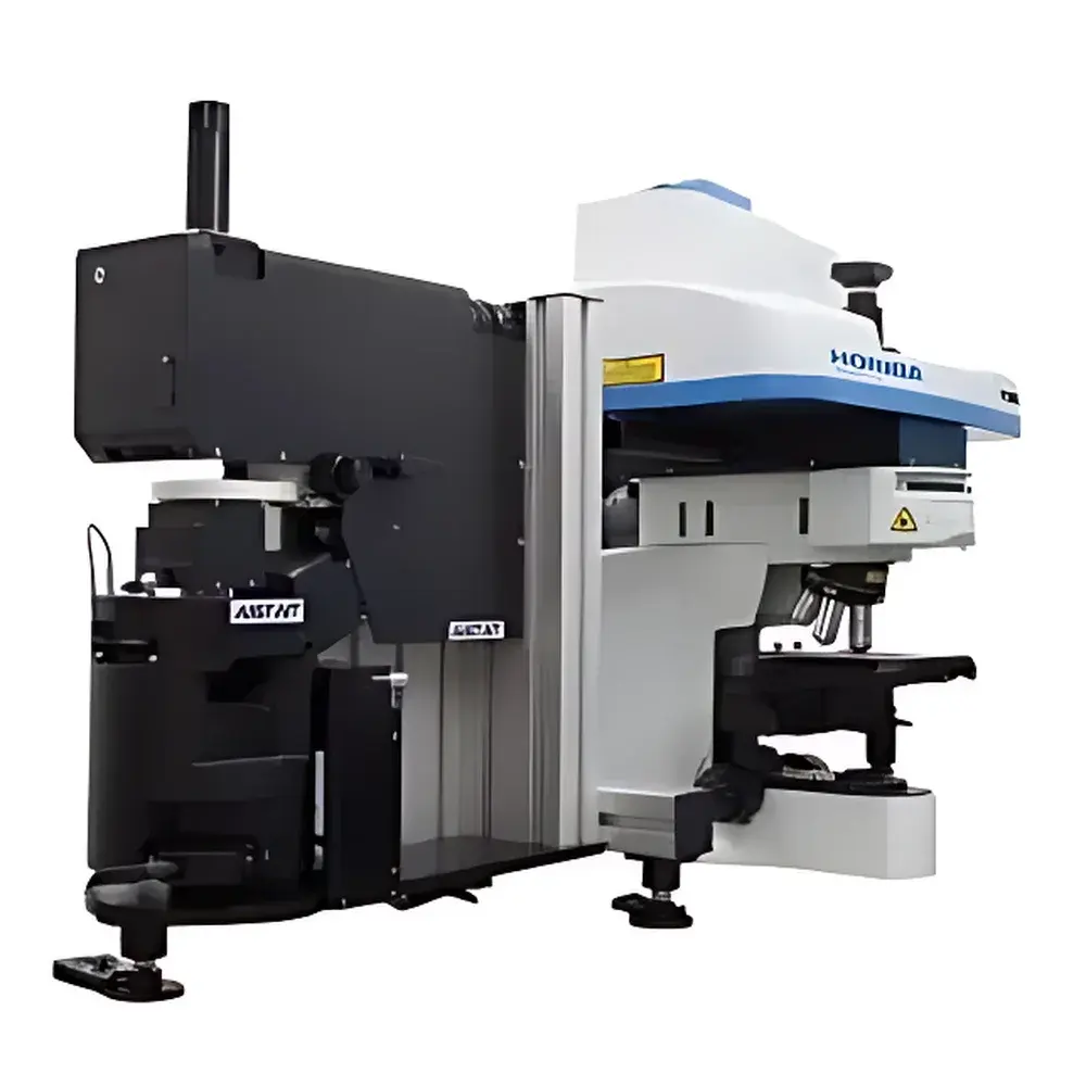
HORIBA XploRA Nano AFM-Raman Coupling System
| Brand | HORIBA |
|---|---|
| Origin | France |
| Model | XploRA Nano |
| Instrument Type | Confocal Micro-Raman Spectrometer |
| Spectral Range | 50–9000 cm⁻¹ |
| Spectral Resolution | 1 cm⁻¹ |
| Spatial Resolution (TERS) | <10 nm |
| Minimum Wavenumber | 50 cm⁻¹ |
| Spectral Reproducibility | <0.1 cm⁻¹ |
Overview
The HORIBA XploRA Nano AFM-Raman Coupling System is an integrated, research-grade platform that synchronously combines atomic force microscopy (AFM) with confocal Raman microspectroscopy to deliver correlative nanoscale structural, mechanical, and chemical characterization. Engineered for precision in hybrid near-field analysis, the system operates on two complementary physical principles: (1) AFM leverages piezoelectric scanning and optical beam deflection to quantify topography, modulus, adhesion, and nanomechanical response at sub-nanometer spatial resolution; and (2) confocal Raman spectroscopy relies on inelastic photon scattering to generate molecular fingerprint spectra—enabling identification of crystal structure, strain, doping level, defect density, and layer stacking in 2D materials, polymers, catalysts, and biological nanostructures. The XploRA Nano uniquely integrates tip-enhanced Raman scattering (TERS) capability, where plasmonic excitation at the AFM tip apex confines optical fields to volumes far below the diffraction limit—achieving chemical mapping with lateral resolution down to <10 nm without compromising spectral fidelity.
Key Features
- True co-localized AFM and Raman imaging: simultaneous acquisition of topographic, mechanical, and vibrational data from identical sample coordinates—eliminating registration error inherent in sequential or post-hoc alignment.
- Optimized TERS architecture: includes plasmonically engineered conductive AFM probes, high-NA (≥0.9) objective lenses (X100), and dual-path illumination (top, side, and bottom coupling) to maximize Raman signal collection efficiency and tip-laser overlap stability.
- Auto-aligned optical lever feedback: real-time compensation of laser beam drift on the AFM photodiode ensures consistent force sensitivity and long-term measurement repeatability during extended spectral mapping sessions.
- High-frequency AFM scanner: low-inertia Z-piezo and XY-scanning stages with active vibration isolation enable stable operation in standard laboratory environments—no dedicated acoustic enclosure required.
- Modular optical interface: supports integration with third-party SPM systems (e.g., Park Systems, Bruker, Nanosurf) via standardized mechanical and electrical interlocks, preserving full functionality of both AFM and spectrometer subsystems.
Sample Compatibility & Compliance
The XploRA Nano accommodates a broad range of solid-state and thin-film samples—including graphene, transition metal dichalcogenides (TMDs), carbon nanotubes, perovskite solar cell layers, semiconductor heterostructures, and biomolecular monolayers—without requiring conductive coating or vacuum conditions. Its confocal design enables depth-resolved Raman profiling in transparent substrates (e.g., SiO₂/Si wafers, glass coverslips), while side-coupled TERS configuration permits chemical analysis of opaque or highly scattering specimens. The system complies with ISO/IEC 17025 requirements for analytical instrument validation and supports GLP/GMP workflows through audit-trail-enabled software logging (21 CFR Part 11 compliant when deployed with HORIBA LabSpec 8 Suite). All optical components meet RoHS and CE directives; laser safety conforms to IEC 60825-1:2014 Class 1/3B depending on configuration.
Software & Data Management
Control and analysis are unified within HORIBA’s LabSpec 8 software platform, which provides synchronized acquisition scripting, real-time spectral preview, multivariate curve resolution (MCR), and hyperspectral image processing (e.g., PCA, cluster analysis, false-color overlay of Raman intensity maps onto AFM height data). Raw AFM and Raman datasets are stored in vendor-neutral formats (JPK .jpk-force, Horiba .hdf5) supporting third-party interoperability with Python-based tools (e.g., SciPy, scikit-learn) and MATLAB. Automated calibration routines include laser wavelength stabilization, grating alignment verification, and spectral shift correction using internal Ne/Ar reference lines—ensuring traceable wavenumber accuracy across multi-day experiments.
Applications
- Layer-number determination and strain mapping in van der Waals heterostructures via G- and 2D-band position shifts correlated with AFM step-height measurements.
- Defect localization in CVD-grown graphene: TERS resolves D/G intensity ratios at grain boundaries with <15 nm precision—complementing conductive-AFM current maps.
- In situ electrochemical Raman-AFM of battery electrode interfaces: monitoring SEI formation kinetics while quantifying local modulus changes during lithiation/delithiation cycles.
- Nanoscale pharmaceutical polymorph identification: distinguishing amorphous vs. crystalline domains in drug-loaded nanoparticles using Raman band deconvolution aligned pixel-by-pixel with phase-imaging AFM contrast.
- TERS-guided nanolithography: using the same tip for localized plasmonic heating and subsequent Raman verification of photochemical modification in polymer resists.
FAQ
What AFM manufacturers are compatible with the XploRA Nano platform?
The system supports OEM integration with major AFM platforms including Bruker Dimension Icon, Park NX10, and Nanosurf FlexAFM—via mechanical docking fixtures and synchronized trigger I/O protocols.
Is TERS performance validated with NIST-traceable standards?
Yes—HORIBA provides TERS resolution verification using Au nanoparticle arrays and graphene edge standards, with documented <10 nm full-width-at-half-maximum (FWHM) in lateral Raman mapping under optimized conditions.
Can the system perform time-resolved Raman-AFM measurements?
LabSpec 8 supports gated acquisition modes synchronized to external stimuli (e.g., voltage pulses, temperature ramps), enabling kinetic studies with temporal resolution limited only by spectrometer readout speed (typically ≥10 ms per spectrum).
Does the XploRA Nano support fluorescence lifetime imaging (FLIM) alongside Raman?
While primarily optimized for Raman and TERS, optional TCSPC modules can be integrated for concurrent FLIM–AFM correlation—subject to separate hardware configuration and licensing.
What maintenance is required for long-term TERS stability?
Routine maintenance includes quarterly alignment verification of the tip-laser overlap using the built-in auto-focus routine and annual recalibration of the spectrometer’s wavelength scale using internal gas lamp references—both fully automated within LabSpec 8.
Related Products
")