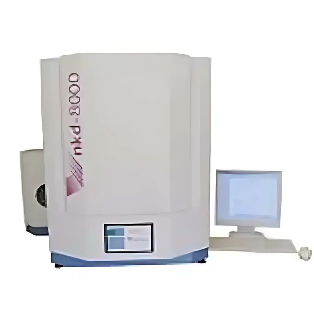
J.A. Woollam NKD8000 Advanced Spectroscopic Ellipsometer System
| Origin | United Kingdom |
|---|---|
| Manufacturer Type | Authorized Distributor |
| Origin Category | Imported Instrument |
| Model | NKD8000 |
| Price | Upon Request |
| Spectral Range (Standard) | 350–1000 nm |
| Spectral Range (UV-Enhanced) | 280–1000 nm |
| Spectral Range (NIR) | 800–1700 nm |
| Spectral Range (Broadband) | 350–1700 nm |
| Spectral Range (Extended Broadband) | 350–2200 nm |
| Spectral Resolution | 1 nm or 2 nm (selectable) |
| Measurement Time | 2–10 minutes (dependent on spectral range and configuration) |
| Analysis Time | 5 seconds–5 minutes (dependent on model complexity) |
| Incident Angle Range | 20°–70° (motorized continuous variable), or fixed angles (30°/50°/70°) |
| Spot Size | 5 mm (standard), 250 µm (optional micro-spot) |
| Sample Stage | X-Y motorized scanning stage (100 mm travel), accommodates samples from 10×10 mm to 200×250 mm |
| Max. Layers | 5-layer stack with up to two unknown parameters per layer |
| Thickness Range | 1 nm – 25 µm (wavelength-, angle-, and polarization-dependent) |
| Accuracy (semi-absorbing films) | thickness <1% (typ.), <3% (max) |
| Accuracy (metallic films) | thickness <1% (typ.), <3% (max) |
| Repeatability | transmission <0.01% (typ.), <0.1% (max) |
| Light Source | 150 W xenon arc lamp (NKD8000v) |
| Power Supply | 220 V, 50 Hz, 2 A or 110 V, 60 Hz, 3 A |
| Dimensions | 890 × 540 × 720 mm |
| Weight | 105 kg |
Overview
The J.A. Woollam NKD8000 Advanced Spectroscopic Ellipsometer System is a high-precision, motorized, broadband optical metrology platform engineered for the non-destructive, contactless characterization of thin-film multilayers and substrates. Based on the fundamental principles of spectroscopic ellipsometry—measuring the change in polarization state (Δ, Ψ) of light upon reflection or transmission—the NKD8000 extends classical ellipsometric capability by integrating simultaneous transmission (T) and reflection (R) spectroscopy across ultraviolet, visible, and near-infrared spectral domains. This dual-channel acquisition ensures intrinsically correlated datasets, eliminating spatial and temporal misalignment errors common in sequential measurement systems. The system operates across multiple spectral configurations—from UV-enhanced (280–1000 nm) to extended broadband (350–2200 nm)—and supports fully automated, software-controlled variable-angle incidence (20°–70° continuous, motor-driven), enabling rigorous dispersion modeling of complex dielectric, polymeric, semiconductor, and metallic thin-film stacks. Designed for R&D laboratories, process development teams, and QC/QA environments in optics, photovoltaics, display technology, and semiconductor manufacturing, the NKD8000 delivers traceable, reproducible determination of refractive index (n), extinction coefficient (k), and physical thickness (d) without sample pre-treatment—even on transparent, semi-transparent, or absorbing substrates.
Key Features
- Simultaneous acquisition of transmission and reflection spectra at identical spatial locations—ensuring direct correlation and eliminating registration drift.
- Motorized, PC-controlled variable-angle incidence (20°–70° continuous), with optional fixed-angle or multi-angle (up to three user-defined positions) configurations.
- Broadband spectral coverage options: standard (350–1000 nm), UV-enhanced (280–1000 nm), NIR (800–1700 nm), broadband (350–1700 nm), and extended broadband (350–2200 nm) with dual-detector architecture.
- Micro-spot option (250 µm diameter) for localized analysis of patterned wafers, microstructures, or heterogeneous surfaces.
- Motorized X-Y scanning stage (100 mm travel) supporting large-area mapping of uniformity, gradient, or defect-related optical property variations.
- Full polarization control: s-polarized, p-polarized, or unpolarized incident light—enabling advanced anisotropy and depolarization analysis.
- Sealed sample chamber with environmental stability—minimizing ambient interference during long-duration or temperature-sensitive measurements.
- Integrated Pro-Optix™ software with editable material database, built-in optical constants libraries, and physics-based regression algorithms for multilayer modeling.
Sample Compatibility & Compliance
The NKD8000 accommodates a broad range of substrate types—including glass, fused silica, silicon, sapphire, polymer films, and flexible substrates—without requiring conductive coatings or vacuum deposition. It supports transparent, semi-transparent, semi-absorbing, and opaque substrates (e.g., metal-backed layers or thick absorbers), provided sufficient signal-to-noise ratio is maintained within the selected spectral window. Film materials include oxides (SiO₂, Ta₂O₅, TiO₂), nitrides (Si₃N₄), polymers (PMMA, PI), chalcogenides, and metals (Al, Cr, Ag, Au). The system meets engineering requirements for ISO/IEC 17025-compliant calibration traceability when used with NIST-traceable reference standards. While not inherently FDA 21 CFR Part 11-certified, its audit trail functionality—including full metadata logging, user authentication, electronic signatures, and version-controlled analysis protocols—supports GLP/GMP-aligned workflows in regulated industries. All optical components conform to RoHS directives and CE electromagnetic compatibility standards.
Software & Data Management
Pro-Optix™ is a modular, Windows-based application providing instrument control, real-time data acquisition, and advanced optical modeling in a single interface. Its core engine implements rigorous least-squares minimization of χ² between measured and modeled Ψ(λ), Δ(λ), T(λ), and R(λ) spectra. Users define multilayer structures via intuitive layer-by-layer construction, assign dispersion models (Cauchy, Sellmeier, Tauc-Lorentz, Drude), and constrain or decouple parameters based on physical plausibility. The software includes automated optimization routines, sensitivity analysis tools, confidence interval estimation, and batch processing for high-throughput sample sets. Raw and processed data are stored in vendor-neutral HDF5 format, with export options to CSV, ASCII, and industry-standard formats (e.g., JPK, IGOR Pro). Audit trails record every user action—including parameter edits, model changes, and result exports—with timestamps and operator IDs. Optional integration with LIMS or MES platforms is supported via OPC UA and RESTful API interfaces.
Applications
- Development and validation of anti-reflective, high-reflection, and bandpass optical coatings for lenses, mirrors, and laser systems.
- Thickness and composition monitoring of ALD and PVD-deposited dielectric stacks in semiconductor front-end-of-line (FEOL) and back-end-of-line (BEOL) processes.
- Characterization of perovskite, CIGS, and organic photovoltaic absorber layers—including degradation kinetics under thermal or illumination stress (with optional heating stage).
- Quantification of surface roughness, interfacial mixing, and density gradients in sol-gel and spin-coated polymer films.
- Optical constant extraction for novel 2D materials (e.g., MoS₂, h-BN) and metamaterial thin-film assemblies.
- Quality assurance of ITO, AZO, and other transparent conductive oxides in display and touch sensor manufacturing.
FAQ
Does the NKD8000 require vacuum operation?
No—measurements are performed in ambient air or nitrogen-purged environments. Vacuum is not required for standard operation, though optional vacuum-compatible stages are available for specialized applications.
Can the system measure films thinner than 1 nm?
Sub-nanometer sensitivity is achievable for high-contrast interfaces (e.g., Si/SiO₂) using enhanced ellipsometric contrast modes; however, routine accuracy below 1 nm typically requires additional hardware such as phase-modulated or rotating-compensator ellipsometry modules.
Is the extended broadband (350–2200 nm) configuration capable of simultaneous UV-VIS-NIR acquisition?
No—the extended configuration uses two physically separate detectors (Si CCD for UV-VIS and InGaAs for NIR), operated sequentially under software coordination. True simultaneous acquisition is limited to overlapping ranges (e.g., 800–1000 nm).
How is calibration verified across the full spectral range?
Calibration is performed using NIST-traceable silicon reference wafers with certified oxide thicknesses, supplemented by spectral irradiance standards (e.g., FEL lamps) and angle verification artifacts. Annual recalibration services are available through J.A. Woollam-certified service centers.
What level of training and technical support is included?
All systems ship with on-site installation, 2-day operator training, and one year of comprehensive software updates and remote diagnostics support. Extended service agreements include priority response, preventive maintenance, and application-specific method development assistance.


