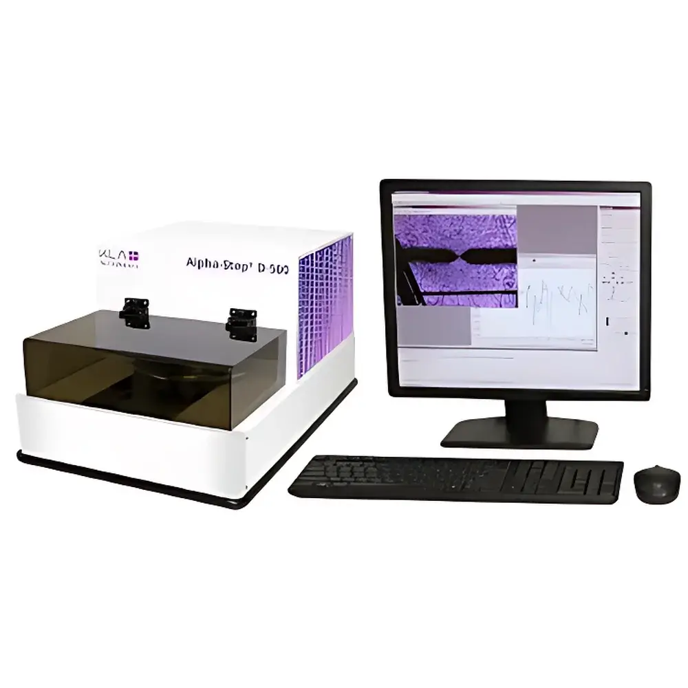
KLA Alpha-Step D-500 Profilometer
| Brand | KLA |
|---|---|
| Origin | Malaysia |
| Model | D-500 |
| Measurement Principle | Contact Stylus Profilometry |
| Vertical Measurement Range | 0.002 µm to 1200 µm |
| Vertical Resolution | Sub-nanometer (typical) |
| Probe Tip Radius | 0.7 µm (standard), optional tips available |
| Normal Force Range | 0.03–15 mg |
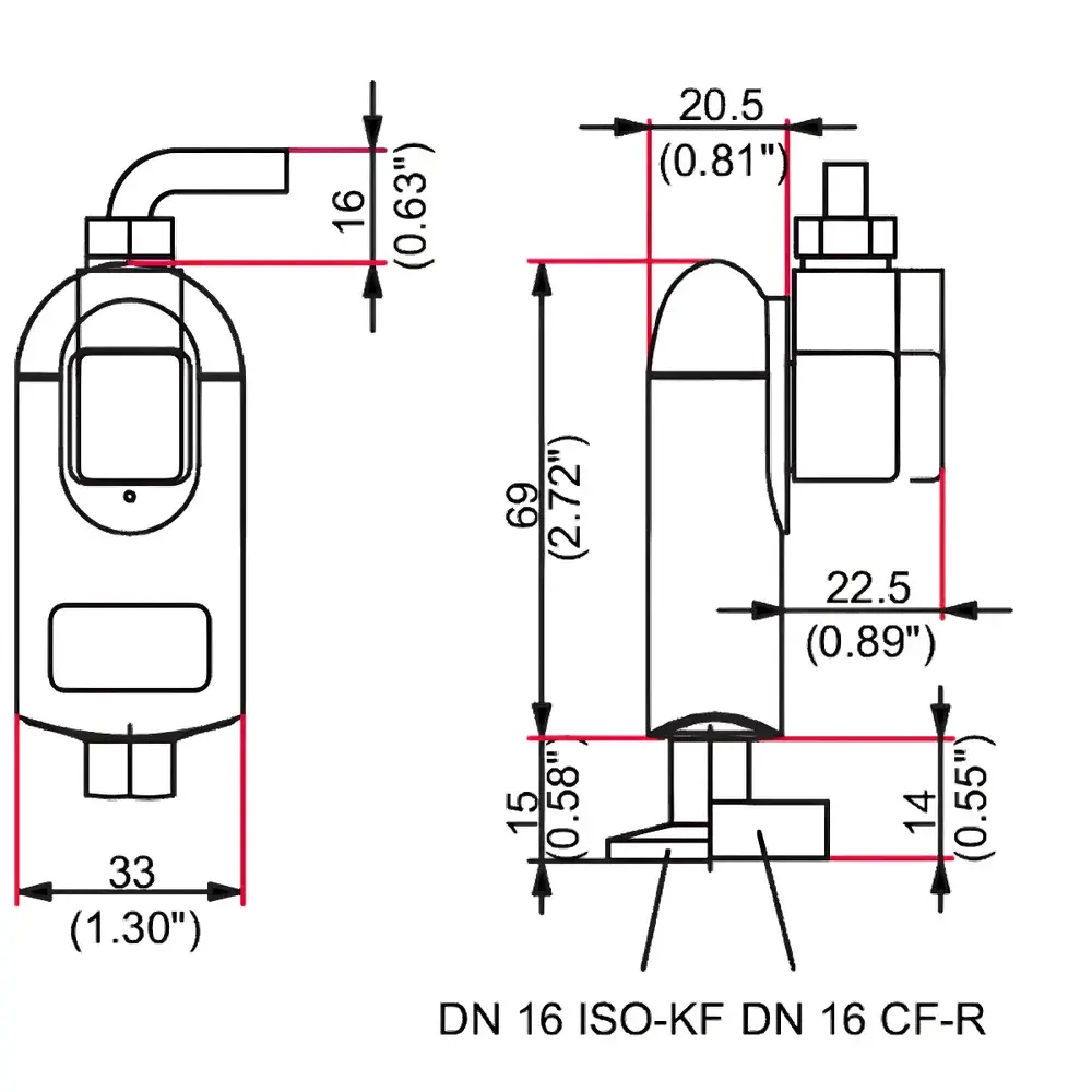
| Scan Length | 55 mm |
| Horizontal Sample Stage | 140 mm manual X-Y stage |
| Max Sample Size | 100 mm × 100 mm |
| Step Height Repeatability | < 0.1% of measured height (RMS) |
| Surface Roughness Parameters | Ra, Rq, Rz, Rt, Rsk, Rku, with ISO 4287/4288 and ASME B46.1 compliant filtering |
| Optical System | Integrated 5 MP color camera with trapezoidal distortion correction and arc error compensation |
| Software | Alpha-Step Analysis Suite with GLP-compliant audit trail, report generation, and 21 CFR Part 11 ready configuration options |
Overview
The KLA Alpha-Step D-500 is a high-precision contact profilometer engineered for quantitative two-dimensional surface topography characterization in research, development, and production environments. Utilizing a calibrated mechanical stylus and optical lever displacement sensing, the D-500 measures vertical surface variations through direct physical interaction—ensuring material-independent traceability across conductive, insulating, soft, or brittle substrates. Its design adheres to fundamental metrology principles defined in ISO 25178-2 (areal surface texture) and ISO 4287 (profile-based roughness), while supporting Stoney equation-based thin-film stress calculation via wafer curvature measurement. With a vertical range spanning from sub-2 nm to 1200 µm and force control down to 0.03 mg, the instrument enables non-destructive profiling of photoresists, low-k dielectrics, MEMS structures, and optoelectronic thin films without deformation artifacts.
Key Features
- Optical lever sensor architecture delivering sub-nanometer vertical resolution and extended dynamic range (0.002 µm–1200 µm) in a single scan
- Adjustable normal force (0.03–15 mg) with real-time feedback, optimized for soft polymers, fragile coatings, and hard ceramics alike
- Interchangeable probe tips—including 0.7 µm radius diamond stylus as standard—with documented tip geometry and wear calibration protocols
- Integrated 5-megapixel color imaging system with real-time trapezoidal distortion correction and arc trajectory compensation for accurate lateral registration
- 140 mm manual X-Y translation stage with fine-positioning verniers and repeatable sample alignment capability
- Compact benchtop footprint (W×D×H ≈ 450 × 520 × 320 mm), suitable for cleanroom integration and space-constrained labs
- Comprehensive error compensation algorithms including thermal drift correction, probe deflection linearity adjustment, and Z-axis hysteresis modeling
Sample Compatibility & Compliance
The D-500 accommodates flat or gently curved samples up to 100 mm × 100 mm and ≤ 25 mm thick. It supports silicon wafers (50–200 mm diameter with adapter kits), glass substrates, metal foils, ceramic tiles, and flexible polymer sheets. All measurements comply with ASTM E1092 (standard practice for profilometer calibration), ISO 21920-2 (geometrical product specifications – surface texture), and USP guidelines for analytical instrument qualification. When configured with audit trail logging, electronic signatures, and user access controls, the system meets FDA 21 CFR Part 11 requirements for regulated environments. Stress measurement mode includes full documentation of Stoney constant derivation, substrate modulus input validation, and curvature fitting residuals per ISO 7500-1.
Software & Data Management
The Alpha-Step Analysis Suite provides an intuitive, workflow-driven interface for acquisition, analysis, and reporting. Raw profilometry data are stored in vendor-neutral HDF5 format with embedded metadata (timestamp, operator ID, calibration certificate ID, environmental conditions). Built-in filters conform to Gaussian, phase-corrected, and spline-based separation per ISO 16610-21 for roughness/waviness partitioning. Statistical process control (SPC) tools calculate Cp/Cpk indices for step height uniformity across die or wafer maps. Reports export to PDF, CSV, or XML with customizable templates aligned to internal SOPs or external standards (e.g., IATF 16949, ISO 9001). Audit logs record every parameter change, file export, or calibration event with immutable timestamps and user attribution.
Applications
- Step Height Metrology: Quantification of etch depth, film thickness (via lift-off or trench fill), CMP removal rates, and lithographic resist development profiles—critical for process window definition in semiconductor front-end-of-line (FEOL) and back-end-of-line (BEOL) fabrication
- Roughness & Waviness Analysis: Surface texture evaluation of polished wafers, sputtered electrodes, evaporated mirrors, and injection-molded optics using Ra, Rq, Rsk, and power spectral density (PSD) metrics
- Wafer Bow & Warp Measurement: Full-scan curvature mapping for stress-induced deformation in multilayer stacks; compatible with stress chuck fixtures for center-supported or edge-clamped configurations
- Film Stress Calculation: Derivation of intrinsic and thermal stress components in PECVD SiNx, ALD Al2O3, or sputtered TiN layers using Stoney’s equation and validated substrate property inputs
- MEMS & Packaging Characterization: Profile verification of cantilevers, comb drives, solder bumps, underfill fillets, and TSV sidewall angles in advanced packaging R&D
FAQ
What is the minimum detectable step height on the D-500?
The system achieves sub-2 nm vertical resolution under optimal conditions (low-noise environment, vibration isolation, stable temperature); practical detection limit for repeatable quantification is ~5 nm RMS for steps ≥ 10 nm in height.
Can the D-500 measure on curved or non-planar substrates?
Yes—within ±2° local surface tilt, provided the curvature radius exceeds 50 mm; automatic tilt correction is applied during scan alignment.
Is probe tip wear monitored automatically?
No real-time wear sensing is implemented; however, the software includes a tip geometry verification routine using reference step standards, and recommended recalibration intervals are tracked via maintenance logs.
Does the system support automated batch measurement?
Manual stage positioning limits fully automated multi-site runs; however, macro scripting (via Python API) enables semi-automated sequences for predefined coordinate sets and analysis protocols.
How is traceability maintained for calibration?
Each instrument ships with NIST-traceable step height and roughness calibration artifacts; calibration certificates document uncertainty budgets per ISO/IEC 17025, and in-house verification uses SRM 1961 and SRM 2101 standards.