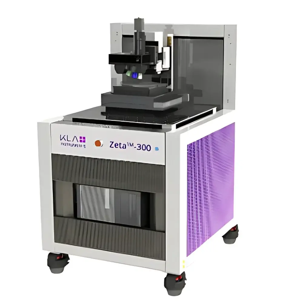
KLA Zeta-300 Non-Contact Optical Profilometer
| Brand | KLA |
|---|---|
| Origin | Malaysia |
| Model | Zeta-300 |
| Product Type | Non-contact profilometer / surface roughness analyzer |
| Measurement Principle | Multi-mode optical interferometry (ZDot™, white-light interferometry, Nomarski differential interference contrast, shear interferometry) |
| Optical Capabilities | Simultaneous high-resolution 3D topography and true-color surface imaging |
| Vertical Resolution | Sub-nanometer (ZIC/ZSI), <0.1 nm (PSI), ≤1 nm (VSI) |
| Step Height Range | 0.8 nm to 1 mm |
| Surface Roughness Range | <0.05 nm RMS to >100 µm Sa |
| Film Thickness Range (ZFT) | 30 nm – 100 µm (transparent films) |
| Defect Detection Limit | ≥1 µm lateral resolution |
| Maximum Sample Size | Up to 280 mm Z-height |
| Compliance | ISO 25178, ISO 4287/4288, ASME B46.1, NIST-traceable calibration standards |
Overview
The KLA Zeta-300 Non-Contact Optical Profilometer is a benchtop 3D surface metrology platform engineered for high-precision, non-destructive characterization of micro- and nano-scale topography, thin-film thickness, and surface defects. Unlike contact stylus profilers or single-mode optical systems, the Zeta-300 integrates six complementary optical measurement technologies—including patented ZDot™, vertical scanning interferometry (VSI), phase-shifting interferometry (PSI), Nomarski differential interference contrast (DIC), shear interferometry (ZSI), and broadband spectral reflectometry (ZFT)—into a unified, software-coordinated architecture. This multi-modal design enables quantitative analysis across an exceptionally broad parameter space: from sub-angstrom smooth surfaces (e.g., polished silicon wafers) to highly reflective, transparent, or low-reflectivity structures (e.g., patterned sapphire substrates, anti-reflective coatings, or MEMS membranes). The system operates on principles of coherent and incoherent light interference, polarization modulation, and spectral phase analysis—each mode selected automatically or manually based on sample optical properties, surface geometry, and required metrological uncertainty.
Key Features
- ZDot™ Technology: Simultaneously acquires high-fidelity 3D topographic data and true-color surface imagery in a single scan—enabling direct correlation between morphology and visual appearance without repositioning.
- Multi-Mode Interferometry Engine: Supports VSI for robust large-step measurement (up to 1 mm), PSI for ultra-high vertical resolution (<0.1 nm) on shallow steps, ZIC for nanoscale slope-sensitive contrast enhancement, and ZSI for Ångström-level quantification without mechanical Z-scanning.
- Integrated ZFT Module: Broadband spectral reflectometer (400–1000 nm) with vertical-incidence illumination, capable of measuring single- and multi-layer transparent film thicknesses from 30 nm to 100 µm—even on surfaces with reflectivity as low as 0.1%.
- Modular Optomechanical Architecture: Interchangeable objective turret (5- or 6-position, manual or motorized), four magnification couplers (0.35× to 1.0×), and application-optimized objectives—including long-working-distance, immersion, transmission, and refractive-index-corrected variants.
- Advanced Motion & Stability Platform: Built-in passive vibration isolation base; optional active air-isolation table; acoustic enclosure standard; piezo-driven Z-stage available for sub-nanometer vertical positioning in ZDot and ZXI modes.
- Automated Workflow Support: Motorized XY stage (150 mm or 200 mm travel), programmable multi-point sequencing, pattern recognition-based auto-alignment, KLARF-compatible defect re-inspection, and NIST-traceable step height and film thickness reference standards.
Sample Compatibility & Compliance
The Zeta-300 accommodates diverse sample classes without physical contact: opaque metals, transparent oxides (SiO₂, ITO), low-reflectivity polymers, structured substrates (PSS, photomasks), flexible PCBs, and fluidic channels. Its optical adaptability ensures reliable measurement on surfaces with varying reflectivity (0.1%–100%), roughness (Sa 100 µm), and step heights (0.8 nm–1 mm). Calibration adheres to ISO 25178-2 (3D surface texture), ISO 4287/4288 (2D profile parameters), and ASME B46.1. All certified reference artifacts—including VLSI-supplied NIST-traceable step standards (8 nm–250 µm) and Si/SiO₂ film thickness standards—are documented per ISO/IEC 17025 requirements. System validation supports GLP and GMP environments via audit-trail-enabled software logging and electronic signature capability compliant with FDA 21 CFR Part 11.
Software & Data Management
The Zeta-300 runs on KLA’s Apex™ software suite—a modular, ISO-compliant analysis environment supporting over 11 languages. Apex implements standardized filtering (Gaussian, Spline, Robust), leveling (least-squares, facet, envelope), and parameter extraction (Sa, Sq, Sz, Rz, Rsk, Rku) aligned with ISO 25178 and ASME B46.1. It generates automated pass/fail reports with user-defined tolerances, overlay annotations, cross-section extraction, and statistical summaries (Cp/Cpk, GR&R). Offline Analysis software replicates full acquisition and processing functionality on external workstations—enabling method development and data review without instrument occupancy. Data export conforms to industry-standard formats (CSV, TIFF, HDF5, STP), and raw interferograms are preserved for traceable reprocessing. Sequence automation includes scriptable macros, KLARF import/export for defect workflows, and integration-ready APIs for factory MES/SPC systems.
Applications
The Zeta-300 serves critical metrology functions across semiconductor front-end and back-end processes—including wafer-level packaging (WLCSP, FOWLP), compound semiconductor epitaxy, LED PSS uniformity verification, and advanced interconnect stress mapping. In MEMS and microfluidics, it quantifies channel depth, sidewall angle, and bonding interface integrity. For medical device manufacturers, it validates surface finish on implant-grade alloys and polymer stents per ISO 10993-24. In academic and national labs, its flexibility supports fundamental research in tribology, thin-film growth kinetics, and nanoscale deformation mechanics. Routine applications include 3D step height metrology (trenches, vias, etch depth), surface roughness and waviness (Ra, Rq, Rz), 2D/3D warpage and film stress (Stoney equation), transparent film thickness uniformity mapping, and automated optical inspection (AOI) with µm-level defect localization and 3D morphological classification.
FAQ
What optical principles underpin the Zeta-300’s multi-mode operation?
The system leverages interference physics across multiple configurations: white-light interferometry (coherence gating), phase-shifting interferometry (temporal phase modulation), Nomarski DIC (polarization-based gradient contrast), shear interferometry (lateral wavefront shearing), and spectral reflectometry (wavelength-dependent phase shift analysis).
Can the Zeta-300 measure transparent films on highly absorbing substrates?
Yes—the ZFT module uses broadband vertical-incidence reflectometry and supports refractive index libraries; it is validated for SiO₂, SiNₓ, photoresists, and polymers on silicon, GaAs, and metal substrates.
Is the system suitable for production-floor deployment?
Yes—its passive vibration isolation, acoustic enclosure, automated multi-point sequencing, and Apex reporting engine support unattended operation in Class 1000 cleanrooms and manufacturing environments with minimal operator intervention.
How is traceability maintained for calibration and measurement uncertainty?
All measurements are referenced to NIST-traceable VLSI standards (step height, film thickness); system performance is verified per ISO 5725 and documented in calibration certificates issued under ISO/IEC 17025-accredited procedures.
Does the Zeta-300 support automated defect re-inspection using KLARF files?
Yes—KLARF import triggers coordinate-based navigation to defect sites; ZDot or ZIC modes then acquire localized 3D morphology and true-color imagery for root-cause analysis.