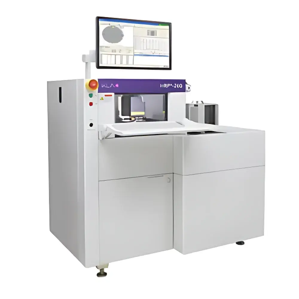
KLA HRP®-260 High-Resolution Contact Profilometer
| Brand | KLA |
|---|---|
| Origin | Malaysia |
| Model | HRP®-260 |
| Product Type | Contact Profilometer / Surface Roughness Tester |
| Operating Principle | Stylus-Based Profilometry |
| Horizontal Scan Range (Long-Range Stage) | 200 mm (no stitching required) |
| High-Resolution Stage Travel | 90 µm × 90 µm |
| Vertical Resolution | 1 nm |
| Stylus Normal Force Range | 0.03–50 mg |
| Step Height Measurement Range | <1 nm to 327 µm |
| Stylus Tip Radius Options | 20 nm – 50 µm |
| Stylus Included | DuraSharp® diamond stylus (40 nm radius) |
| Wafer Handling | Automatic robotic loading for 75–200 mm opaque (e.g., Si, GaAs) and transparent (e.g., sapphire) substrates |
| Compliance | SEMI E4, E5, E30, E37 |
Overview
The KLA HRP®-260 is a high-precision, fully automated contact profilometer engineered for nanoscale surface topography characterization in semiconductor manufacturing, compound semiconductor R&D, LED fabrication, MEMS development, and data storage process control. It operates on the fundamental principle of mechanical stylus scanning—where a diamond-tipped probe traverses the sample surface under precisely controlled normal force, converting vertical displacement into high-fidelity analog voltage signals via a linear variable differential transformer (LVDT) or capacitive sensor architecture. Unlike optical interferometric or confocal systems, the HRP®-260 delivers direct, traceable metrology of step height, roughness, waviness, curvature, and thin-film stress—without ambiguity from optical phase wrapping, coherence artifacts, or reflectivity dependence. Its dual-stage architecture integrates a long-range motorized stage (200 mm travel, no image stitching) with a piezoelectric high-resolution stage (90 µm × 90 µm scan area, 1 nm positioning resolution), enabling seamless transition between macro-scale wafer-level inspection and sub-micron feature profiling—functionally bridging the performance gap between conventional stylus profilometry and atomic force microscopy (AFM).
Key Features
- Dual-stage scanning system: Combines 200 mm continuous horizontal travel with 90 µm × 90 µm piezoelectric XY stage for AFM-grade lateral resolution and nanometer-level vertical repeatability.
- Ultra-low-force stylus control: Programmable normal force range from 0.03 mg to 50 mg ensures minimal sample deformation while maintaining signal-to-noise integrity across soft polymers, hard dielectrics, and brittle III-V materials.
- Integrated optical navigation: Co-located low-magnification (1×–5×) and high-magnification (20×–100×) objectives with 5 MP digital camera enable rapid feature identification, precise stylus placement, and real-time visual verification without stage repositioning.
- Advanced arc correction algorithm: Compensates for parabolic trajectory-induced measurement error during curved-scan motion—critical for accurate step height quantification on non-planar or warped wafers.
- Automated wafer handling: Robotic arm supports unattended loading/unloading of 75–200 mm wafers—including opaque (Si, GaAs) and transparent (sapphire, quartz) substrates—with integrated alignment sensors and SECS/GEM-compliant communication.
- SEMI-compliant factory integration: Fully supports SEMI E4 (equipment communications), E5 (GEM), E30 (data collection), and E37 (process job management) standards for SPC linkage, remote diagnostics, and host-driven recipe execution.
Sample Compatibility & Compliance
The HRP®-260 accommodates a broad spectrum of substrate types and geometries, including silicon, gallium arsenide, silicon carbide, sapphire, fused silica, and patterned glass wafers up to 200 mm in diameter. Vacuum chucks ensure flat, vibration-damped mounting for standard planar wafers; three-point stress chucks enable precise bow and warp measurement per ASTM F390 and ISO 14406. For highly curved or bowed substrates, optional flexure-compensating stages maintain probe contact integrity throughout full-field scans. All measurements are traceable to NIST-certified step height standards (VLSI Standards, 8 nm–100 µm), and software implements ISO 4287 (surface roughness), ISO 4288 (lay and waviness assessment), and ASME B46.1 (surface texture parameters). Data acquisition and reporting comply with FDA 21 CFR Part 11 requirements when configured with audit trail, electronic signature, and role-based access controls.
Software & Data Management
The system runs KLA’s Apex Analysis Software—a modular, Windows-based platform supporting both real-time measurement and offline analysis. Apex includes ISO-compliant filtering (Gaussian, 2RC, spline), advanced leveling (least-squares, facet, polynomial), and quantitative extraction of step height, roughness (Sa, Sq, Sz), waviness, curvature radius, and residual stress (via Stoney equation integration). Custom pass/fail criteria, multi-layer report generation (PDF, CSV, XML), and 11-language UI support streamline global deployment. Offline software licenses allow full recipe development, simulation, and historical data reprocessing without consuming tool uptime. Graphical pattern recognition—trained on user-defined fiducials—enables robust, repeatable alignment across tools and shifts, significantly improving inter-tool correlation (ITC) and reducing setup time. All raw and processed datasets are stored with full metadata (timestamp, operator ID, calibration status, environmental logs) to satisfy GLP/GMP documentation requirements.
Applications
The HRP®-260 serves as a primary metrology tool for process development and high-volume manufacturing control. Key use cases include: quantifying etch depth and deposition thickness in gate-last CMOS processes; measuring photoresist line edge roughness (LER) and sidewall angle post-lithography; characterizing epitaxial layer uniformity in GaN-on-sapphire LED structures; evaluating MEMS device release etch profiles and stiction risk; validating spin-on-glass planarization in advanced packaging; and correlating defect morphology (e.g., particles, scratches, residues) with electrical failure modes. In R&D environments, its high-resolution stage enables rapid screening of novel thin-film stacks, nanoimprint lithography fidelity, and stress evolution during thermal cycling—providing quantitative feedback for TCAD model validation.
FAQ
What is the difference between the HRP®-260 and the P-260?
The HRP®-260 shares the same core measurement engine and automation capabilities as the P-260 but adds a high-resolution piezoelectric XY stage (90 µm × 90 µm, 1 nm resolution) for sub-micron feature characterization—effectively extending its utility into AFM-equivalent spatial regimes.
Can the HRP®-260 measure transparent substrates like sapphire?
Yes—its integrated optical imaging system supports auto-alignment and stylus positioning on both opaque (e.g., Si) and transparent (e.g., sapphire, quartz) wafers using contrast-based feature detection and backside illumination options.
Is the system compatible with existing HRP®-240/250 infrastructure?
Yes—KLA offers a documented upgrade path that includes new electronics (USB interface), Windows-based controller, updated Apex software, high-res camera, and 23″ display—retaining legacy fixtures while delivering ~2× faster throughput on five-point measurement routines.
How is traceability ensured for production-critical measurements?
Traceability is maintained through NIST-traceable VLSI step height standards, in situ calibration routines, and software-enforced version-controlled measurement protocols—all logged with full audit trail per 21 CFR Part 11.
What stylus options are available for high-aspect-ratio trench metrology?
Stylus tip radii range from 20 nm to 50 µm, and included angles span 20°–100°; DuraSharp® 40 nm radius, 90° stylus is recommended for production-grade step height and LER measurement on sub-100 nm features.