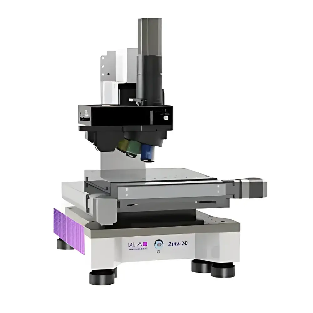
KLA Zeta-20 Non-Contact Optical Profilometer
| Brand | KLA |
|---|---|
| Origin | Malaysia |
| Model | Zeta-20 |
| Product Type | Non-contact Profilometer / Surface Roughness Analyzer |
| Measurement Principle | Multi-Mode Optical Interferometry (ZDot™, White-Light Interferometry, Nomarski DIC, Shear Interference), Spectral Reflectometry |
| Key Capabilities | 3D Topography, True-Color Imaging, Step Height (0.008 nm – 10 mm), Surface Roughness (Ra down to sub-Å), Film Thickness (30 nm – 100 µm), Automatic Defect Detection (>1 µm), Wafer-Scale Warpage & Stress Analysis |
Overview
The KLA Zeta-20 Non-Contact Optical Profilometer is a benchtop, multi-modal 3D surface metrology system engineered for precision characterization of micro- and nano-scale topographic features across R&D and high-volume manufacturing environments. Unlike single-principle profilometers, the Zeta-20 integrates six complementary optical measurement technologies—including proprietary ZDot™, vertical scanning interferometry (VSI), phase-shifting interferometry (PSI), Nomarski differential interference contrast (DIC), shear interferometry (ZSI), and broadband spectral reflectometry (ZFT)—within a single robust architecture. This convergence enables quantitative, non-destructive analysis of diverse sample types: transparent and opaque substrates, low-reflectivity (90%) surfaces, nanosmooth films and highly textured structures, and multilayer stacks with varying refractive indices. The system operates on the principle of optical path difference detection via coherent or incoherent light interference, calibrated against NIST-traceable step height and film thickness standards. Its modular design supports full traceability under ISO/IEC 17025, ASTM E2921 (for thin-film thickness), ISO 25178 (for 3D surface texture), and USP (for pharmaceutical surface quality), making it suitable for GLP/GMP-compliant laboratories.
Key Features
- ZDot™ Technology: Simultaneously acquires high-resolution 3D topography and true-color surface imaging in a single scan—enabling correlation of morphological structure with optical appearance.
- Multi-Mode Interferometry: Combines VSI (for 100 nm–100 µm steps), PSI (sub-Å resolution on smooth surfaces), and ZSI (8 nm–80 nm steps without Z-scanning) to cover an unprecedented dynamic range of vertical scales.
- ZFT Module: Integrated broadband spectrometer (400–1000 nm) performs model-based fitting of reflectance spectra to determine film thickness from 30 nm to 100 µm—even on ultra-low-reflectivity solar cell textures (<0.1% R).
- Automated Defect Inspection (AOI): Detects, classifies, and spatially maps defects ≥1 µm; integrates KLARF file support for coordinate-driven re-inspection and 3D defect profiling (height, volume, edge slope).
- Full-Wafer & Macro-Scale Metrology: Motorized XY stages (up to 300 mm travel) enable stitching of >100×100 mm² areas; optional tilt stage supports edge profiling of HDD platters and solar wafers.
- Apex™ Analysis Software: Implements ISO 25178-2, ASME B46.1, and DIN 4768 surface parameters; supports custom filtering (Gaussian, S-filter), stress calculation via Stoney’s equation, and automated pass/fail reporting with multi-language UI (11 languages).
Sample Compatibility & Compliance
The Zeta-20 accommodates samples ranging from 10 mm × 10 mm dies to full 300 mm wafers, including fragile MEMS devices, polymer microfluidic chips, bioengineered microneedle arrays, and compound semiconductor heterostructures. Its high-dynamic-range illumination (dual white LED + optional dark-field and back-lighting) ensures stable signal acquisition on challenging surfaces: silicon nitride anti-reflective coatings, silver busbars on photovoltaic cells, copper RDL layers beneath transparent photoresist, and low-k dielectrics. All measurement modes comply with industry audit requirements: data integrity is maintained through time-stamped audit trails, electronic signatures, and 21 CFR Part 11–ready configuration (when deployed with validated Apex software). Calibration is performed using VLSI-certified NIST-traceable standards—8 nm–250 µm step height artifacts and Si/SiO₂ reference wafers with certified 270 nm oxide thickness.
Software & Data Management
The Zeta-20 runs on KLA’s unified Apex platform, which unifies instrument control, real-time analysis, and report generation. Sequence programming supports fully automated workflows: graphic recognition aligns patterned wafers; multi-point measurement routines execute predefined coordinate lists; and stitching algorithms merge adjacent fields into gigapixel-scale topographic datasets. Offline analysis software replicates all on-tool functionality, enabling method development and retrospective analysis without instrument downtime. Data export adheres to industry formats: .zdf (native binary), .xyz (ASCII point cloud), .tif (georeferenced height maps), and .csv (statistical summaries). All raw and processed data are stored with metadata including operator ID, timestamp, environmental conditions (optional sensor integration), and calibration history—ensuring full traceability per ISO 17025 Clause 7.7.
Applications
- Semiconductor Packaging: Measures Cu pillar height, photoresist thickness, UBM roughness, and bump coplanarity in WLCSP/FOWLP processes—without damaging soft resist layers.
- Photovoltaics: Quantifies pyramid texture depth (Ra, Rz), Ag finger height/volume, isolation trench depth, and SiNx antireflective coating uniformity across 156 mm wafers.
- PCB & Flexible Electronics: Characterizes solder mask thickness, blind via depth, conductor edge profile, and surface roughness of rolled-annealed copper foils.
- Microfluidics & Biotech: Profiles channel cross-sections, quantifies bonding interface flatness, measures sealed cavity depth with refractive index compensation, and resolves microneedle tip geometry.
- Data Storage: Inspects HDD platter edge bevel angle, detects edge chipping or contamination, and verifies ramp clearance specifications.
- Laser Processing: Validates ablation depth/width in scribing, marking, and structuring applications—on Si, GaAs, glass, and polyimide substrates.
FAQ
What vertical resolution can the Zeta-20 achieve?
Sub-ångström vertical resolution is attainable using PSI on atomically flat surfaces; ZSI delivers ≤0.08 nm RMS noise on 1–80 nm steps; ZDot provides ~0.1 nm height repeatability for steps >50 nm.
Can the Zeta-20 measure transparent films on reflective substrates?
Yes—ZFT uses spectral reflectometry with material dispersion models to decouple substrate and film contributions; ZDot leverages polarization-sensitive contrast for direct visualization and quantification.
Is the system compatible with cleanroom environments?
Standard configurations meet Class 1000 (ISO 6) requirements; optional laminar flow enclosures and ESD-safe components are available for Class 100 (ISO 5) deployment.
How does the Zeta-20 handle highly sloped or curved surfaces?
Tilt-adjustable stages and motorized rotation enable oblique-angle illumination; advanced algorithms correct for perspective distortion and defocus during stitching and curvature modeling.
What documentation supports regulatory submissions?
KLA provides IQ/OQ/PQ protocols, uncertainty budgets per GUM (JCGM 100), and validation packages aligned with FDA, ICH, and ISO 13485 requirements for medical device and pharma applications.