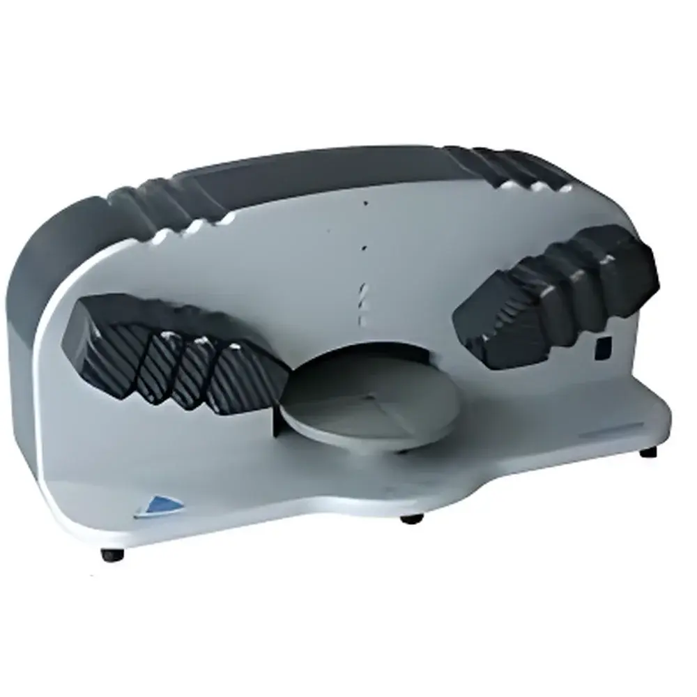
SpecEl-2000-VIS Ellipsometer by SP Spectral Products
| Brand | SP Spectral Products |
|---|---|
| Origin | USA |
| Manufacturer Type | Authorized Distributor |
| Import Status | Imported |
| Model | SpecEl-2000-VIS |
| Wavelength Range | 380–780 nm (standard), 450–900 nm (optional) |
| Optical Resolution | 4.0 nm FWHM |
| Angle of Incidence | 70° |
| Spot Size | 2 mm × 4 mm (standard), 200 µm × 400 µm (optional) |
| Thickness Measurement Range | 0.1 nm – 5 µm (single transparent film) |
| Thickness Resolution | 0.1 nm |
| Refractive Index Accuracy | ±0.005% |
| Measurement Time | 3–15 s (per acquisition) |
| Dynamic Acquisition Interval | 3 s |
| Mechanical Height Tolerance | ±1.5 mm |
| Angular Tolerance | ±1.0° |
| Maximum Layer Count | 32 layers |
| Software Platform | Windows-based 32-bit control and analysis suite |
Overview
The SpecEl-2000-VIS is a precision spectroscopic ellipsometer engineered for non-destructive, contactless characterization of thin-film optical properties on solid substrates. Operating on the fundamental principles of polarization modulation and phase-difference analysis, it quantifies the change in the state of polarized light upon reflection from a sample surface—enabling simultaneous determination of film thickness, complex refractive index (n + iκ), and extinction coefficient across the visible spectrum. Designed for laboratory-scale R&D and process development environments, the system integrates a stabilized broadband light source, a high-stability dual-rotating compensator optical train, and a calibrated CCD-based spectrometer. Its fixed 70° angle of incidence ensures optimal sensitivity for dielectric and semiconductor thin films while maintaining robust signal-to-noise performance under ambient lab conditions.
Key Features
- Fixed-angle (70°) spectroscopic ellipsometry configuration optimized for high signal fidelity and repeatability in the visible range (380–780 nm standard; 450–900 nm optional)
- Sub-nanometer thickness resolution (0.1 nm) and refractive index accuracy of ±0.005%, validated against NIST-traceable reference standards
- Configurable spot size: standard 2 mm × 4 mm for macro-area averaging or micro-spot option (200 µm × 400 µm) for localized analysis on patterned wafers or heterostructures
- Real-time data acquisition with minimum cycle time of 3 seconds—enabling dynamic monitoring of deposition, etching, or annealing processes
- Modular optical architecture with factory-aligned rotating polarizer and analyzer stages, minimizing alignment drift over extended operation
- Comprehensive mechanical stability: angular tolerance ≤ ±1.0° and vertical height tolerance ≤ ±1.5 mm, ensuring measurement consistency across multi-day campaigns
Sample Compatibility & Compliance
The SpecEl-2000-VIS supports flat, rigid substrates up to 150 mm in diameter, including silicon wafers, fused silica, glass slides, and metal-coated coupons. It accommodates single-layer and multilayer stacks (up to 32 layers) comprising dielectrics (SiO₂, Si₃N₄, Al₂O₃), semiconductors (Si, Ge, a-Si), transparent conductive oxides (ITO, AZO), and organic thin films (PEDOT:PSS, perovskites). All measurements comply with ASTM E1939–21 (Standard Guide for Spectroscopic Ellipsometry) and ISO 15382:2020 (Optics and photonics — Spectroscopic ellipsometers — Vocabulary and parameters). The instrument’s calibration protocol aligns with GLP documentation requirements and supports audit-ready reporting for regulated QC/QA workflows.
Software & Data Management
Controlled via a dedicated Windows-based 32-bit application, the SpecEl software provides full instrument orchestration—including motorized stage positioning, spectral acquisition, regression modeling, and library-assisted optical constant fitting. Data files are stored in HDF5 format with embedded metadata (wavelength grid, incidence angle, instrument ID, timestamp, user annotation), ensuring FAIR (Findable, Accessible, Interoperable, Reusable) compliance. Export options include CSV, XML, and industry-standard JPK/SE format for cross-platform compatibility with third-party modeling tools (e.g., CompleteEASE, WVASE). Audit trail functionality logs all parameter changes, model selections, and fit iterations—meeting FDA 21 CFR Part 11 requirements when deployed in GMP-regulated environments.
Applications
- Development and validation of anti-reflective, high-reflection, and beam-splitter coatings for optical components
- In-line monitoring of PVD, CVD, ALD, and spin-coated film growth kinetics in semiconductor fabrication
- Characterization of passivation layers (e.g., Al₂O₃ on silicon solar cells) for photovoltaic efficiency optimization
- Quantitative analysis of degradation mechanisms in OLED encapsulation barriers and perovskite absorber layers
- Refinement of dispersion models (Cauchy, Sellmeier, Tauc-Lorentz) for novel metamaterial and plasmonic thin-film systems
- Thickness uniformity mapping across 4-inch and 6-inch wafers using motorized XY translation stage (optional)
FAQ
What wavelength ranges does the SpecEl-2000-VIS support?
The standard configuration covers 380–780 nm (visible spectrum); an optional upgrade extends coverage to 450–900 nm for near-IR applications.
Can the system measure absorbing or opaque films?
Yes—it determines complex optical constants (n and k) for both transparent and weakly absorbing films (e.g., metals <10 nm thick, doped oxides); quantitative k-value extraction requires appropriate model constraints during regression.
Is vacuum or nitrogen purging required for operation?
No—optical path is sealed and purged internally; ambient-air operation is fully supported without performance compromise in the visible range.
How many layers can be modeled simultaneously?
The software supports optical modeling of up to 32 discrete layers, including substrate, interfacial roughness zones, and graded interfaces.
Does the system include calibration standards?
Yes—a certified Si/SiO₂ reference wafer with traceable oxide thickness (±0.05 nm) is supplied for daily verification and instrument validation.


