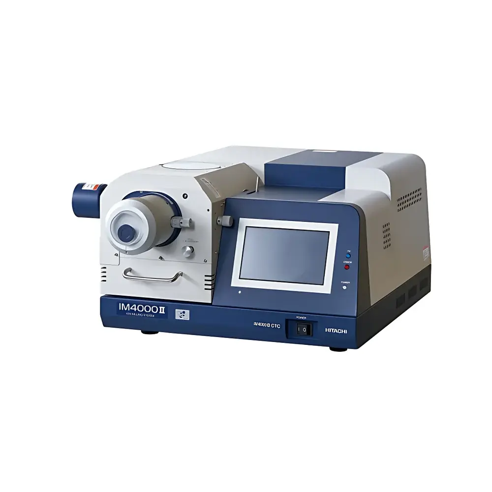
Hitachi IM4000 II Ion Milling System
| Brand | Hitachi |
|---|---|
| Origin | Japan |
| Manufacturer | Hitachi High-Tech Corporation |
| Type | Imported Instrument |
| Model | IM4000 II |
| Pricing | Available Upon Request |
Overview
The Hitachi IM4000 II Ion Milling System is a high-precision, dual-mode sample preparation instrument engineered for electron microscopy (EM) applications. It operates on the principle of broad-beam argon ion sputtering—accelerating inert gas ions toward a solid sample surface to remove material via physical sputtering. This non-chemical, low-damage technique enables artifact-free cross-sectional and planar surface preparation essential for transmission electron microscopy (TEM), scanning electron microscopy (SEM), and focused ion beam (FIB)-SEM correlative workflows. Unlike conventional mechanical polishing or chemical etching, ion milling preserves crystalline integrity, minimizes amorphization, and eliminates preferential etching—critical for analyzing grain boundaries, interfacial layers, thin films, and heterogeneous composites. The IM4000 II builds upon the legacy of Hitachi’s E-3500 platform with a redesigned ion gun architecture that delivers higher current density and improved beam collimation, directly enhancing milling throughput and reproducibility.
Key Features
- Dual-Mode Operation: Seamlessly switch between cross-section milling (for subsurface structural imaging) and planar milling (for large-area surface uniformity), both fully programmable via intuitive front-panel interface.
- Optimized Ion Gun Design: Features an enhanced LaB6-based ion source and electrostatic lens system, achieving up to 300 µm/h sputter rate on single-crystal silicon—reducing typical cross-section preparation time by 66% versus the E-3500 model.
- Modular Sample Stage: A fully detachable, motorized tilt-and-rotate stage allows precise positioning of irregular or multi-component samples prior to loading into the vacuum chamber; facilitates rapid edge definition and reproducible incident-angle alignment.
- High-Stability Vacuum Architecture: Integrated turbomolecular pumping system maintains base pressure <1×10⁻⁵ Pa during operation, minimizing contamination and ensuring consistent ion beam energy distribution.
- Real-Time Process Monitoring: Equipped with integrated quartz crystal microbalance (QCM) and Faraday cup diagnostics for in situ sputter rate calibration and endpoint detection.
Sample Compatibility & Compliance
The IM4000 II accommodates a wide range of conductive and non-conductive materials—including metals, ceramics, semiconductors, geological specimens, and polymer composites—without requiring conductive coating. Its low-energy ion beam (<10 keV) and variable incidence angle (0°–90°) minimize topographic artifacts and thermal damage, making it suitable for temperature-sensitive biological hybrids and layered oxide structures. The system complies with ISO 14644-1 Class 5 cleanroom-compatible design standards for vacuum chamber construction and meets electromagnetic compatibility (EMC) requirements per IEC 61326-1. All operational parameters—including beam voltage, current, tilt angle, and milling duration—are logged with timestamped metadata, supporting GLP/GMP-aligned documentation and audit readiness per FDA 21 CFR Part 11 when integrated with validated LIMS environments.
Software & Data Management
Controlled via Hitachi’s proprietary IM-Manager software suite, the IM4000 II supports full recipe-based automation, including multi-step sequences with conditional logic (e.g., pause at defined depth, auto-adjust angle after threshold removal). All process logs—including vacuum history, ion current stability profiles, and stage position trajectories—are exported in CSV and XML formats compatible with laboratory information management systems (LIMS). Audit trails record user ID, timestamp, parameter changes, and system alerts—enabling traceability required under ISO/IEC 17025 and ASTM E2821-12 guidelines for EM sample preparation validation.
Applications
- Preparation of TEM lamellae from bulk semiconductor wafers and advanced packaging substrates
- Generation of artifact-free cross-sections for failure analysis of solder joints, Cu/low-k interconnects, and MEMS devices
- Planar milling of geological thin sections for cathodoluminescence (CL) and electron backscatter diffraction (EBSD) mapping
- Surface deconvolution of multilayer optical coatings and photovoltaic absorber stacks
- Interface characterization in battery electrode/electrolyte systems and solid-state electrolyte composites
FAQ
What vacuum level does the IM4000 II achieve during operation?
The system reaches a base pressure of ≤1×10⁻⁵ Pa using a combination of turbo-molecular and scroll pumps, ensuring stable ion beam performance and minimal hydrocarbon contamination.
Can the IM4000 II be used for insulating samples without carbon or metal coating?
Yes—the instrument supports charge compensation via flood gun integration (optional accessory), enabling stable milling of oxides, glasses, and polymers without conductive overlayer deposition.
Is remote monitoring or integration with SEM/FIB platforms supported?
While standalone operation is standard, RS-232 and Ethernet interfaces enable OEM-level protocol integration; Hitachi provides API documentation for third-party automation frameworks compliant with SEM/FIB workflow orchestration standards.
How is calibration verified for quantitative depth profiling?
Calibration is performed using certified reference materials (e.g., NIST SRM 2053 SiO2/Si bilayers); sputter yield values are stored per material class and automatically applied during recipe generation.


