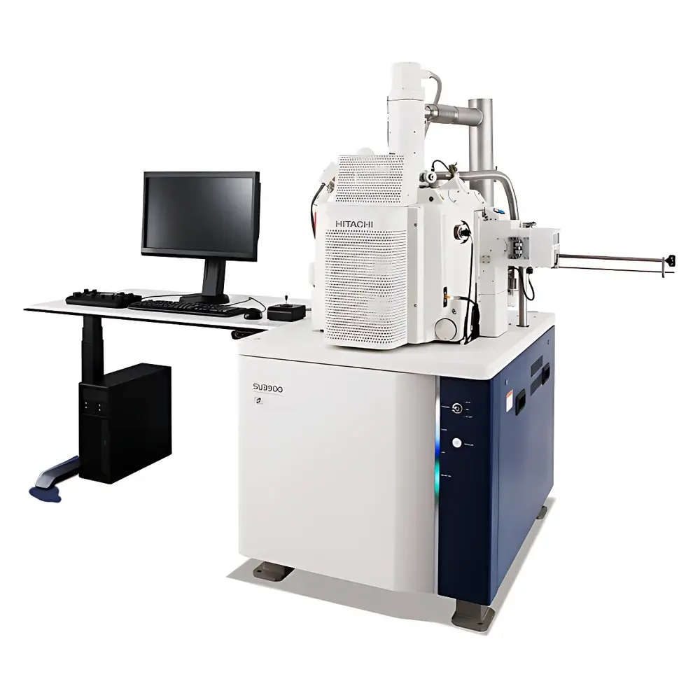
Hitachi SU3900 Large-Volume Scanning Electron Microscope
| Brand | Hitachi |
|---|---|
| Origin | Japan |
| Manufacturer | Hitachi High-Tech Corporation |
| Product Type | Imported |
| Model | SU3900 |
| Electron Source | Tungsten Filament |
| Secondary Electron Resolution | 3.0 nm |
| Magnification Range | ×5–300,000 (standard mode), ×7–800,000 (high-magnification mode) |
| Accelerating Voltage | 0.3–30 kV |
| Backscattered Electron Resolution | 4.0 nm @ 30 kV (low-vacuum mode) |
| Maximum Sample Diameter | 300 mm |
| Maximum Sample Height | 130 mm |
| Maximum Sample Weight | 5 kg |
| Navigation Field of View | up to Ø200 mm |
Overview
The Hitachi SU3900 is a high-performance, large-volume scanning electron microscope (SEM) engineered for industrial and advanced materials laboratories requiring direct, non-destructive analysis of oversized and heavy specimens. Unlike conventional SEMs constrained by limited stage travel and sample chamber dimensions, the SU3900 integrates a robust mechanical architecture with an ultra-large specimen chamber—designed specifically to accommodate samples up to 300 mm in diameter, 130 mm in height, and 5 kg in mass—without necessitating sectioning, trimming, or mounting compromises. Its operation relies on thermionic emission from a tungsten filament electron source, delivering stable beam current over extended acquisition periods. The system supports dual-mode imaging: secondary electron (SE) detection for high-surface-topography contrast at 3.0 nm resolution, and backscattered electron (BSE) detection for compositional contrast with 4.0 nm resolution at 30 kV in low-vacuum conditions. Accelerating voltage is continuously adjustable from 0.3 kV to 30 kV, enabling optimal signal-to-noise balance across conductive, semi-conductive, and insulating materials—including as-received metal components, castings, battery electrodes, and composite laminates.
Key Features
- Large-Specimen Compatibility: Standard chamber accommodates samples up to Ø300 mm × 130 mm × 5 kg—2.5× greater mass capacity than predecessor models—eliminating pre-analysis machining for automotive parts, turbine blades, PCB assemblies, and geological cores.
- Extended Field-of-View Navigation: Integrated SEM MAP navigation system combines multi-angle CCD imaging with stage rotation and automated image stitching to generate seamless, high-fidelity overview maps up to Ø200 mm—enabling precise region-of-interest targeting without manual repositioning.
- Multi-Zigzag Imaging: Automated high-magnification mosaic acquisition across user-defined areas; individual frames are geometrically aligned and pixel-registered to produce gigapixel-scale composite images suitable for grain boundary mapping, coating uniformity assessment, and defect density quantification.
- Intelligent Filament Technology (IFT): Real-time tungsten filament health monitoring algorithm estimates remaining operational life based on emission stability, cumulative beam-on time, and vacuum history—providing predictive maintenance alerts and minimizing unplanned interruptions during long-duration particle size distribution (PSD) or EDS mapping sessions.
- One-Touch Imaging Workflow: Fully automated alignment routines—including gun alignment, stigmator correction, focus, brightness/contrast optimization, and astigmatism compensation—reduce time-to-image after sample loading to under 90 seconds, supporting high-throughput QA/QC environments.
Sample Compatibility & Compliance
The SU3900 is validated for use with both conductive and non-conductive specimens under high-vacuum and low-vacuum modes (down to 10 Pa), accommodating uncoated polymers, ceramics, biological tissues, and oxidized metals. Its chamber design complies with ISO 14644-1 Class 5 cleanroom integration standards and supports optional accessories including cryo-transfer stages, heating/cooling holders (−180°C to +1000°C), and integrated energy-dispersive X-ray spectrometers (EDS) meeting ASTM E1508 and ISO 22309 requirements for elemental microanalysis. All vacuum interlocks, high-voltage safety circuits, and emergency stop logic conform to IEC 61010-1:2010 and UL 61010-1 certification protocols. Data acquisition workflows support GLP/GMP audit trails per FDA 21 CFR Part 11 when paired with compliant LIMS or ELN platforms.
Software & Data Management
Operation is managed via Hitachi’s proprietary “SEM Suite” software—a Windows-based application supporting DICOM-compliant image export, TIFF/PNG/JPEG2000 multi-layer output, and HDF5-formatted raw data containers for post-acquisition processing. The platform includes built-in measurement tools adhering to ISO 16700 (particle analysis), ASTM E1245 (inclusion rating), and ISO 13565 (surface roughness profiling). All instrument parameter logs, operator actions, timestamped image metadata, and calibration records are stored in tamper-evident SQLite databases with configurable retention policies. Remote diagnostics and firmware updates are conducted over TLS 1.2-encrypted connections, and role-based access control (RBAC) ensures separation of duties between operators, supervisors, and service engineers.
Applications
- Automotive & aerospace quality assurance: In-situ inspection of brake rotors, weld zones, and additive-manufactured turbine vanes without sectioning.
- Electronics failure analysis: Cross-sectional imaging of full-size PCBs, wafer-level packages, and flexible displays using low-kV SE imaging to minimize charging artifacts.
- Geoscience and mining: Textural characterization of drill core segments, ore mineral assemblages, and porosity networks in reservoir rock samples.
- Battery R&D: Cathode/anode particle morphology, SEI layer thickness estimation, and dendrite growth tracking across full electrode coupons (up to 10 cm × 10 cm).
- Medical device validation: Surface topography verification of orthopedic implants, porous scaffolds, and drug-eluting stent coatings under low-vacuum conditions.
FAQ
What vacuum modes does the SU3900 support, and what are their typical applications?
The SU3900 operates in high-vacuum mode (10⁻³–10⁻⁴ Pa) for maximum resolution on conductive samples and low-vacuum mode (10–133 Pa) for charge-free imaging of insulators and hydrated specimens—ideal for uncoated polymers, biological sections, and ceramic powders.
Can the SU3900 be integrated with EDS or WDS systems?
Yes—the instrument features standardized flanges and electrical interfaces compatible with third-party and Hitachi-branded EDS detectors (e.g., Horiba EX-350, Oxford X-MaxN), and optional wavelength-dispersive spectrometers meeting ISO 16615 analytical precision requirements.
Is remote operation supported for multi-site laboratories?
Full remote control—including stage navigation, image acquisition, and parameter adjustment—is enabled via secure VNC-over-HTTPS with two-factor authentication; session logs are automatically archived per internal SOPs.
How does Intelligent Filament Technology reduce operational downtime?
IFT continuously evaluates filament emission decay kinetics and predicts end-of-life within ±8 hours; notifications trigger scheduled maintenance windows, preventing mid-acquisition filament burnout during overnight EDS mapping or time-lapse corrosion studies.
Does the SU3900 meet regulatory requirements for pharmaceutical manufacturing environments?
When configured with audit-trail-enabled software, electronic signatures, and calibrated reference standards traceable to NIST SRMs, the SU3900 satisfies FDA 21 CFR Part 11, EU Annex 11, and PIC/S GMP Annex 11 documentation integrity criteria for materials release testing.


