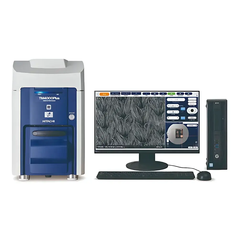
Hitachi TM4000PlusIII / TM4000III Desktop Scanning Electron Microscope
| Brand | Hitachi |
|---|---|
| Origin | Japan |
| Manufacturer Type | Original Equipment Manufacturer (OEM) |
| Product Category | Imported Instrument |
| Model | TM4000PlusIII / TM4000III |
| Instrument Type | Benchtop SEM |
| Electron Source | Tungsten Filament |
| Accelerating Voltage | 5 kV, 10 kV, 15 kV, 20 kV |
| Magnification Range | 10× – 100,000× (photographic magnification) |
| Maximum Sample Diameter | 80 mm |
| Maximum Sample Thickness | 50 mm |
| Stage Travel | X: 40 mm, Y: 35 mm |
| Vacuum Mode | Standard Low-Vacuum Operation |
| Automation Features | Auto-focus, Auto-brightness/contrast, Filament Usage Monitoring, Programmable Workflow Sequencing, Integrated Particle Analysis Support (with Oxford AZtecLiveLite) |
Overview
The Hitachi TM4000PlusIII and TM4000III are benchtop scanning electron microscopes (SEM) engineered for high-reproducibility imaging and elemental analysis in resource-constrained laboratories. Designed around a thermionic tungsten filament electron source and optimized low-vacuum operation, these instruments eliminate the need for conductive coating of non-conductive samples—enabling direct observation of polymers, ceramics, biological tissues, powders, and composites without carbon or gold sputtering. The system operates at accelerating voltages of 5–20 kV, balancing surface detail resolution with reduced charging artifacts and minimized beam damage. With a photographic magnification range from 10× to 100,000×, the TM4000PlusIII/TM4000III delivers consistent sub-micron morphological characterization suitable for routine quality control, academic teaching, materials R&D, and failure analysis workflows. Its compact footprint (≤0.5 m² floor space) and simplified vacuum architecture reduce infrastructure requirements—no external cooling water, high-power electrical supply, or dedicated vibration-isolation tables are needed.
Key Features
- Low-vacuum imaging mode (10–100 Pa) enabling uncoated, insulating sample observation without charging artifacts
- Integrated auto-focus and auto-brightness/contrast algorithms for one-button image acquisition—reducing operator dependency and training time
- Filament usage monitoring system that estimates remaining filament life and provides proactive replacement alerts—supporting multi-user lab scheduling and preventive maintenance planning
- Enhanced beam current capability in TM4000PlusIII configuration, compatible with Oxford Instruments’ AZtecLiveLite software for automated particle detection, classification, and size distribution analysis
- Programmable workflow engine allowing full automation of stage movement (X/Y), magnification switching, image capture, and detector synchronization—ideal for batched sample screening or standardized QC protocols
- Robust mechanical stage with 40 mm (X) × 35 mm (Y) travel range and precise motorized positioning—supporting reproducible region-of-interest navigation across heterogeneous specimens
Sample Compatibility & Compliance
The TM4000PlusIII/TM4000III accommodates specimens up to 80 mm in diameter and 50 mm in height, accommodating standard petri dishes, filter membranes, circuit board fragments, and metallurgical cross-sections. Its low-vacuum environment supports hydrated, outgassing, or temperature-sensitive samples—making it suitable for applications aligned with ASTM E1508 (Standard Guide for Quantitative Analysis by Energy Dispersive Spectroscopy) and ISO 16700 (Electron probe microanalysis — Quantitative analysis using energy-dispersive X-ray spectrometry). While not certified for GLP or GMP environments out-of-the-box, audit-ready operation is achievable through optional logging modules and user-accessible metadata tagging (e.g., timestamped acquisition parameters, operator ID, instrument state). Firmware updates comply with IEC 61000-6-3 (EMC emissions) and IEC 61010-1 (safety requirements for electrical equipment).
Software & Data Management
Hitachi’s proprietary SEM Control Software (v4.x) provides intuitive GUI-based operation with customizable toolbars, real-time histogram-based contrast optimization, and DICOM-compliant image export (JPEG, TIFF, BMP). AZtecLiveLite integration enables automated particle analysis—including morphology-based thresholding, convex hull measurement, and cumulative size distribution reporting per ISO 9276-2. All image and parameter metadata—including kV, WD, dwell time, magnification, vacuum status, and filament hours—are embedded in EXIF headers. Raw data files support post-acquisition reprocessing (e.g., contrast stretching, FFT filtering) without loss of original signal fidelity. Audit trail functionality records user login/logout events, parameter changes, and image save actions—facilitating compliance with FDA 21 CFR Part 11 when deployed with network-authenticated accounts and encrypted storage.
Applications
- Materials science: Fractography of alloys, dispersion analysis of nanocomposites, coating thickness evaluation via cross-sectional imaging
- Electronics manufacturing: Solder joint inspection, PCB trace integrity verification, contamination identification on wafer surfaces
- Pharmaceutical QA: API particle morphology assessment, excipient blend uniformity validation, tablet coating defect mapping
- Geoscience & mining: Mineral phase identification, porosity quantification in core samples, grain boundary analysis in sedimentary rocks
- Academic education: Hands-on SEM training for undergraduate labs; correlative light-SEM exercises using shared sample holders
FAQ
Is the TM4000PlusIII compatible with EDS detectors from vendors other than Oxford Instruments?
Yes—while AZtecLiveLite is fully validated and supported, the system provides standard analog and digital output interfaces (LVDS, USB 3.0) for third-party EDS hardware integration, subject to firmware compatibility verification.
Can the instrument operate under high-vacuum conditions for higher-resolution imaging?
No—the TM4000PlusIII/TM4000III is designed exclusively for low-vacuum and variable-pressure operation; it does not support high-vacuum (<10⁻³ Pa) imaging modes.
What is the typical filament lifetime under standard operating conditions?
Tungsten filaments typically deliver 100–150 hours of cumulative beam-on time depending on accelerating voltage and current settings; the built-in monitoring system tracks actual usage and projects end-of-life within ±10% accuracy.
Does the programmable workflow feature support conditional logic (e.g., “if feature detected, increase magnification”)?
No—workflow sequencing is linear and deterministic; it executes pre-defined positional, magnification, and acquisition steps without real-time image-based decision branching.
Is remote operation supported via LAN or VPN?
Yes—full remote desktop control is enabled via secure RDP over local networks; cloud-based access requires on-premise gateway configuration and IT policy alignment.


