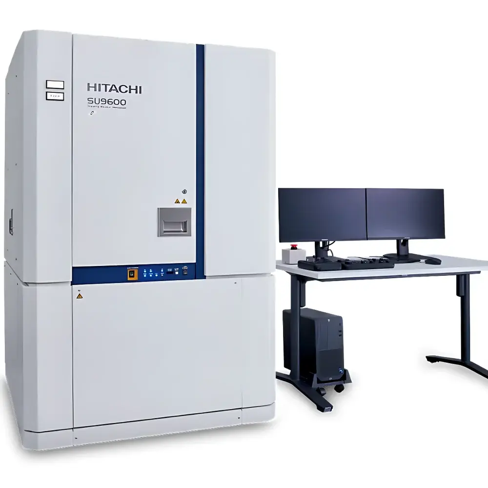
Hitachi SU9600 Ultra-High-Resolution Cold Field-Emission Scanning Electron Microscope
| Brand | Hitachi |
|---|---|
| Origin | Japan |
| Manufacturer | Hitachi High-Tech Corporation |
| Type | Floor-Standing SEM |
| Electron Source | Cold Field-Emission Gun (CFEG) |
| Resolution | 0.6 nm @ 1 kV, 0.4 nm @ 30 kV (Secondary Electron Imaging) |
| Magnification Range | 80× to 3,000,000× |
| Accelerating Voltage | 0.01–30 kV |
Overview
The Hitachi SU9600 is an ultra-high-resolution cold field-emission scanning electron microscope engineered for sub-nanometer morphological characterization in advanced semiconductor process development, next-generation battery materials, 2D nanomaterials, and quantum device fabrication. Built upon Hitachi’s legacy of CFEG-based SEM innovation since 1972, the SU9600 integrates a newly optimized cold field-emission electron source with an aberration-minimized in-lens objective design and ExB secondary electron detection architecture. This configuration enables stable, high-brightness electron beam delivery across the full accelerating voltage range (10 V–30 kV), supporting both low-voltage surface-sensitive imaging (e.g., polymer interfaces, insulating thin films) and high-energy bulk structural analysis. The instrument operates on conventional high-vacuum SEM principles—electron beam rastering over conductive or metallized specimens, with signal generation via secondary electron (SE), backscattered electron (BSE), and transmitted electron (STEM-in-SEM) detection pathways—while delivering reproducible 0.4 nm resolution at 30 kV and 0.6 nm at 1 kV under standard operating conditions.
Key Features
- In-Lens Objective Design: Short focal length electromagnetic lens integrated within the pole piece minimizes spherical and chromatic aberrations, enabling consistent sub-nanometer resolution across magnifications and accelerating voltages.
- ExB Secondary Electron Detector: Orthogonal electric and magnetic fields above the objective lens separate and guide low-energy SEs without perturbing the primary beam trajectory—enhancing signal collection efficiency, contrast, and signal-to-noise ratio (SNR), especially at low probe currents and low kV.
- Advanced Cold Field-Emission Gun (CFEG): Newly engineered CFEG delivers superior beam stability, brightness, and energy spread (<0.3 eV) over extended acquisition periods—critical for long-duration EDS mapping, automated wafer inspection, and sequential STEM imaging.
- VCD Backscattered Electron Detector: A newly developed scintillator-based BSE detector (Variable Contrast Detector) provides rapid positional feedback and enhanced atomic-number contrast with improved temporal response for real-time navigation and region-of-interest (ROI) targeting.
- High-Definition Imaging Engine: Supports pixel resolutions up to 40,960 × 30,720 (1.25 Gpixel), with adjustable dwell time ranging from 10 ns to 100 µs per pixel—enabling adaptive signal optimization for heterogeneous samples and beam-sensitive materials.
Sample Compatibility & Compliance
The SU9600 accommodates standard 3”–8” wafers, TEM grids, bulk metal/ceramic sections, and coated non-conductive specimens (e.g., polymers, biological tissues). Optional stage configurations support tilt (±90°), rotation (360°), and heating/cooling (−180°C to +1000°C) for in situ experiments. All vacuum systems comply with ISO 27427 (vacuum integrity), IEC 61000-6-3 (EMC), and JIS C 61326-1 (laboratory equipment safety). For regulated environments—including semiconductor fabs and pharmaceutical R&D labs—the system supports audit-ready operation through optional GLP/GMP-compliant software modules with 21 CFR Part 11–enabled electronic signatures, user access control, and full audit trail logging.
Software & Data Management
Operation is managed via Hitachi’s EM Flow Creator platform—a modular, scriptable GUI that unifies hardware control, image acquisition, automated workflow sequencing, and metadata embedding. Predefined templates enable one-click alignment, focus/stigmation, and multi-point survey mapping; custom Python-based macros allow integration with external metrology tools (e.g., CD-SEM overlay analysis, AI-driven defect classification pipelines). Raw image data are stored in standardized TIFF/DM3 formats with embedded calibration metadata (pixel size, kV, WD, dwell time, detector type). Export options include HDF5 for machine learning training datasets and CSV-compatible reports for LIMS integration. Remote monitoring and diagnostics are supported via secure TLS-encrypted web interface.
Applications
- Semiconductor metrology: Critical dimension (CD) verification, gate oxide uniformity, EUV resist morphology, and finFET sidewall roughness quantification.
- Advanced materials: Grain boundary analysis in solid-state electrolytes, catalyst nanoparticle dispersion, MXene layer stacking fidelity, and graphene edge topology.
- Life sciences: Cryo-SEM of vitrified cellular structures, immunogold labeling localization, and correlative light-EM (CLEM) sample registration.
- Failure analysis: Cross-sectional void detection in Cu/low-k interconnects, solder joint intermetallic growth kinetics, and delamination propagation in 3D IC stacks.
- Quality assurance: Automated foreign material identification (FIB-SEM correlation ready), coating thickness validation, and particulate contamination screening per ISO 14644-1 Class 5 cleanroom protocols.
FAQ
What vacuum level is required for optimal cold field-emission performance?
The SU9600 maintains <1×10⁻⁸ Pa in the gun chamber and <5×10⁻⁴ Pa in the specimen chamber during operation—achieved via differential pumping with ion getter and turbo-molecular pumps.
Is the SU9600 compatible with energy-dispersive X-ray spectroscopy (EDS)?
Yes—fully integrated with Hitachi’s AZtecLive EDS system, supporting simultaneous high-speed elemental mapping at ≤10 nm spatial resolution with live spectrum imaging and phase identification.
Can the SU9600 perform automated particle analysis on large-area scans?
Yes—via EM Flow Creator’s Particle Analysis Module, which executes threshold-based segmentation, size/shape distribution statistics, and exportable reports compliant with ASTM E1245 and ISO 13322-2.
Does the system support beam deceleration mode for surface-sensitive imaging?
Yes—retarding field optics enable landing energies as low as 10 eV while maintaining 1 kV gun voltage, reducing charging and surface damage on insulators without compromising resolution.
What service and calibration documentation is provided for regulatory audits?
Each system ships with a NIST-traceable calibration certificate, IQ/OQ documentation package, and optional PQ validation support aligned with ISO/IEC 17025 and FDA guidance for analytical instrument qualification.


