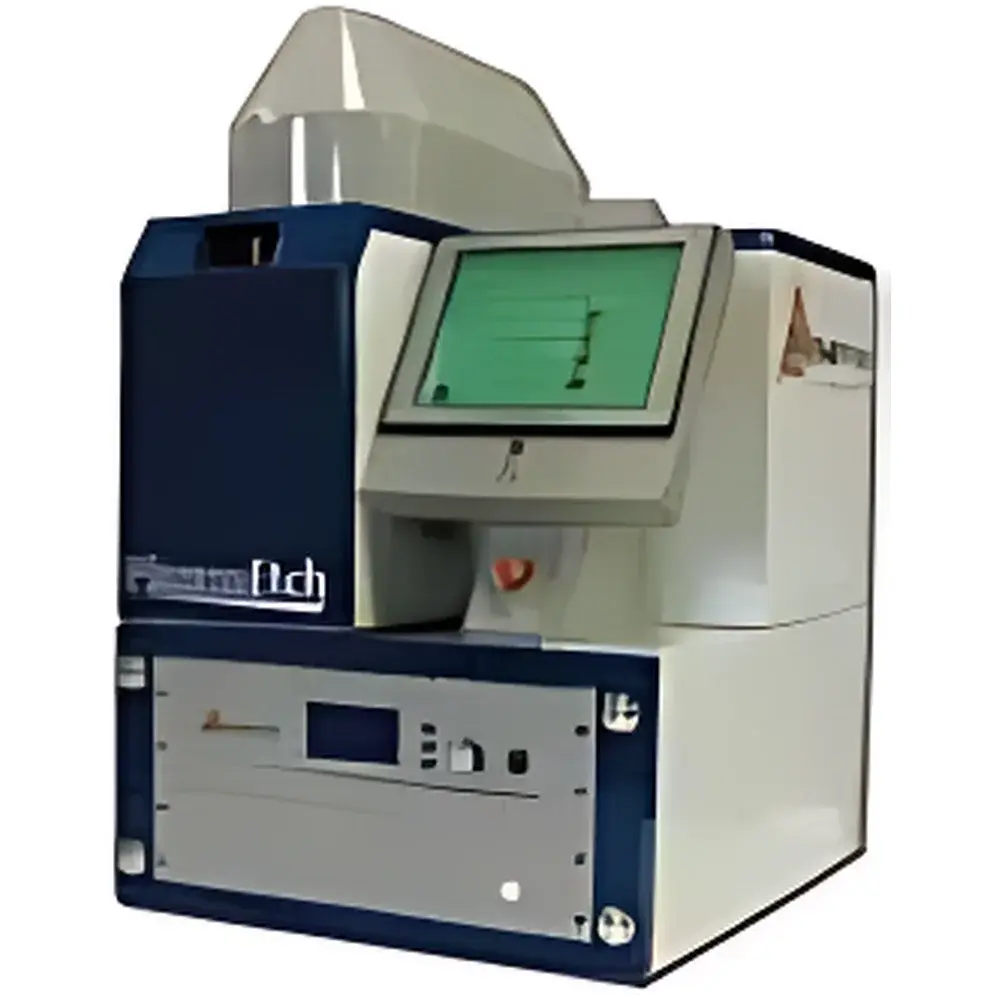
Nisene PlasmaEtch Plasma Decapsulation System
| Brand | Nisene |
|---|---|
| Origin | USA |
| Manufacturer Type | Authorized Distributor |
| Origin Category | Imported |
| Model | PlasmaEtch |
| Pricing | Available Upon Request |
Overview
The Nisene PlasmaEtch Plasma Decapsulation System is a precision-engineered, microwave-excited, downstream plasma etching instrument designed exclusively for non-destructive semiconductor package decapsulation. Unlike traditional wet chemical or mechanical deprocessing methods, PlasmaEtch utilizes a chemically selective, low-energy, ion-free plasma generated from process gases (e.g., O₂, CF₄, SF₆, or custom gas blends) to isotropically remove mold compounds—including epoxy resins, silicone gels, and polyimide-based encapsulants—while preserving delicate bond wires (Au, Cu, Ag), die surfaces, and underlying metallization. The system operates via radical-driven surface reaction kinetics rather than physical sputtering or high-energy ion bombardment, enabling high selectivity (>500:1) between organic encapsulant and metallic or silicon substrates. This principle ensures minimal thermal stress (<40 °C substrate temperature), no X-ray or UV radiation emission, and zero residual chemical contamination—making it suitable for failure analysis (FA), reliability testing, counterfeit detection, and reverse engineering in ISO/IEC 17025-accredited labs.
Key Features
- Downstream microwave plasma source with tunable power (300–1500 W) and precise gas flow control via mass flow controllers (MFCs) for O₂, CF₄, Ar, and other reactive/inert gases
- Isotropic etch profile with uniform material removal across complex 3D package geometries—including QFN, BGA, WLCSP, stacked-die, and fan-out packages
- Programmable etch recipes supporting multi-step gas sequencing, timed ramping, and real-time endpoint monitoring via optical emission spectroscopy (OES) integration capability
- Temperature-controlled sample stage (ambient to 60 °C) with active cooling to maintain sub-40 °C die surface during extended etch cycles
- Integrated safety interlocks compliant with UL 61010-1 and IEC 61000-6-4; fully enclosed chamber with vacuum-tight quartz viewing port and remote operation interface
- Chemical-free operation—no acids, solvents, or hazardous waste generation—meeting RoHS, REACH, and EPA Tier II environmental compliance requirements
Sample Compatibility & Compliance
PlasmaEtch accommodates substrates up to 150 mm × 150 mm and handles diverse packaging configurations: leadframe-based (SOIC, QFP), laminate-based (BGA, CSP), wafer-level (WLP), and advanced heterogeneous integration assemblies. It is validated for decapsulation of copper-wire-bonded devices (including oxidized Cu), silver wire bonds (a known challenge for conventional plasma systems), and aluminum ribbon bonds without wire lifting, necking, or intermetallic degradation. The process meets ASTM F2150-22 (“Standard Guide for Failure Analysis of Microelectronic Devices”) and supports GLP/GMP-aligned documentation workflows. Full audit trail logging—including recipe parameters, gas flows, pressure profiles, duration, operator ID, and timestamp—is available for FDA 21 CFR Part 11-compliant environments when paired with optional software modules.
Software & Data Management
The system runs on embedded Linux-based control firmware with a touchscreen HMI and optional Ethernet/RS-232 connectivity. Standard software includes recipe library management, real-time process parameter visualization (pressure, forward/reflected power, gas flow rates), and CSV export of session logs. Optional FA-Link™ software enables integration with SEM/FIB workstations and LIMS platforms, supporting automated report generation with embedded images, spectral data, and metadata traceability per ISO/IEC 17025 clause 7.8. All software modules undergo annual cybersecurity validation per NIST SP 800-53 Rev. 5 controls.
Applications
- Non-destructive delidding of IC packages prior to optical inspection, SEM cross-sectioning, or X-ray tomography
- Preparation of samples for EDS, EBIC, or nano-FTIR analysis where surface integrity and elemental purity are critical
- Failure root cause analysis of moisture-induced corrosion, void formation, or bond wire fatigue
- Counterfeit IC detection through visual verification of die markings, layout authenticity, and metallization structure
- Process development support for new encapsulation materials (e.g., low-k mold compounds, halogen-free epoxies)
- Qualification of advanced packaging technologies including 2.5D/3D ICs, chiplets, and heterogeneous SiP assemblies
FAQ
What types of bond wires are compatible with PlasmaEtch decapsulation?
Gold, copper (bare and oxidized), silver, aluminum, and palladium-coated wires have been validated across >12,000 production runs with no observable wire damage or interfacial delamination.
Can PlasmaEtch remove filled epoxy mold compounds containing silica or alumina?
Yes—typical removal rate is ~200 µm/hour for standard 70% silica-filled EMC; higher filler loadings may require adjusted gas ratios and extended dwell time, but full removal remains achievable without substrate erosion.
Is operator training required before system deployment?
Nisene provides on-site installation qualification (IQ), operational qualification (OQ), and comprehensive technician certification covering safety protocols, recipe optimization, maintenance scheduling, and troubleshooting—typically completed within two business days.
Does the system support automated endpoint detection?
While not standard, optional OES integration enables real-time spectral monitoring of CO, CO₂, or CF emission lines to infer polymer breakdown onset; endpoint can be triggered programmatically based on intensity thresholds or derivative analysis.
What vacuum and gas supply infrastructure is needed?
A roughing pump (≤1 × 10⁻² mbar base pressure) and clean, oil-free compressed air (for pneumatic actuators) are required; process gases must be supplied via dedicated stainless-steel lines with dual-stage regulators and particulate filters meeting CGA G-4.1 standards.


