Bruker Dimension FASTSCAN Atomic Force Microscope (AFM/SPM/STM)
| Brand | Bruker |
|---|---|
| Origin | USA |
| Manufacturer Type | Authorized Distributor |
| Origin Category | Imported |
| Model | Dimension FASTSCAN |
| Pricing | Available Upon Request |
Overview
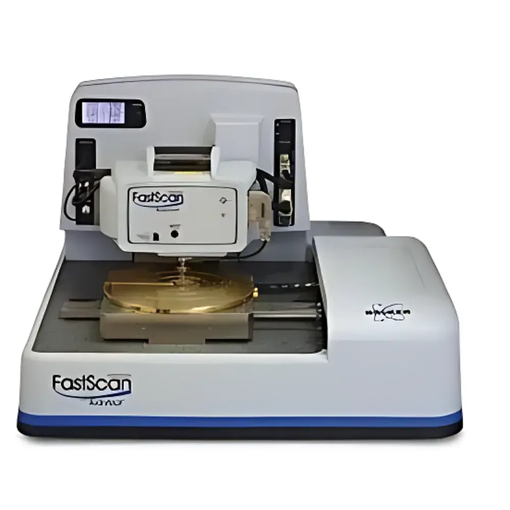
The Bruker Dimension FASTSCAN Atomic Force Microscope (AFM) is a high-speed, research-grade scanning probe microscope engineered for quantitative nanoscale surface characterization in air, liquid, and controlled environments. Leveraging Bruker’s proprietary FastScan™ technology—developed from the legacy of Digital Instruments and Veeco—the system operates on the fundamental principle of dynamic force detection via laser Doppler interferometry and photodiode-based deflection sensing. Unlike conventional AFMs limited by mechanical resonance constraints and piezoelectric scanner bandwidth, the FASTSCAN platform integrates a dual-stage scanner architecture with optimized feedback control algorithms and low-noise electronics to achieve real-time imaging at frame rates exceeding 125 Hz without compromising spatial resolution or measurement fidelity. This enables true video-rate acquisition of topographical, phase, amplitude, and force-distance data—making it uniquely suited for dynamic processes such as polymer crystallization, electrochemical interface evolution, biomolecular conformational changes, and nanomechanical property mapping under operational conditions.
Key Features
- Dual-stage scanner design: High-bandwidth XY stage combined with precision Z actuator for sub-angstrom vertical resolution and <1 nm lateral resolution in tapping and contact modes
- Real-time imaging up to 125 Hz frame rate—enabling single-second AFM image acquisition in ambient and liquid environments
- Integrated optical microscope (10×–50× zoom) with motorized focus and LED illumination for precise tip-sample navigation and region-of-interest targeting
- Modular probe holder compatible with standard commercial cantilevers (e.g., AC240TS, RTESPA, SNL-10), supporting multiple operational modes including TappingMode™, PeakForce Tapping®, Contact Mode, and Force Spectroscopy
- Robust environmental enclosure options for vibration isolation, acoustic damping, and temperature/humidity stabilization (optional)
- Pre-aligned, factory-calibrated laser path and photodetector assembly ensuring consistent signal-to-noise ratio across instrument lifetime
Sample Compatibility & Compliance
The Dimension FASTSCAN accommodates a broad range of sample geometries and materials—from rigid silicon wafers and metallic thin films to soft hydrogels, lipid bilayers, and live cells cultured on glass or mica substrates. Sample height tolerance extends up to 15 mm; maximum sample diameter is 150 mm. The system complies with international safety standards including IEC 61010-1 (electrical safety), ISO 14644-1 Class 5 cleanroom compatibility (when equipped with optional enclosure), and meets electromagnetic compatibility requirements per FCC Part 15 and CE directives. For regulated environments, Bruker provides documentation packages supporting GLP/GMP audit readiness, including IQ/OQ protocols and traceable calibration records aligned with ISO/IEC 17025 guidelines.
Software & Data Management
Acquisition and analysis are managed through Bruker’s NanoScope Analysis v2.0 software suite, which supports full 32-bit/64-bit Windows OS platforms and features native HDF5 file format export for long-term archival and cross-platform interoperability. The software includes automated tip qualification routines, real-time FFT spectral monitoring, batch processing workflows, and scripting interfaces (Python API) for custom algorithm integration. Audit trail functionality logs all user actions—including parameter modifications, scan start/stop timestamps, and calibration events—in accordance with FDA 21 CFR Part 11 requirements when enabled. Raw data files retain metadata for environmental conditions (temperature, humidity), scanner calibration coefficients, and feedback loop settings—ensuring full experimental reproducibility.
Applications
- Semiconductor metrology: Line edge roughness (LER), critical dimension (CD) analysis, and defect review on advanced logic and memory wafers
- Materials science: Nanomechanical property mapping (modulus, adhesion, dissipation) of composites, 2D materials (graphene, MoS₂), and perovskite thin films
- Life sciences: In situ structural dynamics of membrane proteins, amyloid fibril growth kinetics, and cellular response to pharmacological stimuli
- Data storage R&D: Bit-pattern fidelity assessment on heat-assisted magnetic recording (HAMR) media and patterned media templates
- Quality control labs: Routine surface roughness (Sa, Sq, Sz) quantification per ISO 25178 and ASTM E2922 standards
FAQ
What scanning modes does the Dimension FASTSCAN support?
TappingMode™, PeakForce Tapping®, Contact Mode, Lateral Force Microscopy (LFM), Phase Imaging, Amplitude Modulation, and Force-Distance Spectroscopy—with optional modules for electrical (CAFM, KPFM) and magnetic (MFM) characterization.
Is the system compatible with in-situ electrochemical cells?
Yes—Bruker offers certified electrochemical AFM (EC-AFM) cells with integrated potentiostat interfaces and corrosion-resistant fluidic manifolds for operando studies of battery electrode interfaces and catalyst surfaces.
Can the FASTSCAN be upgraded to include nanomechanical mapping capabilities?
Absolutely—the system supports seamless integration of PeakForce QNM™ and HarmoniX™ modules for quantitative nanomechanical property extraction, including elastic modulus, deformation, and adhesion histograms.
Does Bruker provide application-specific training and method development support?
Yes—Bruker Field Application Scientists deliver on-site installation qualification, hands-on user training, and application-specific protocol development tailored to semiconductor, academic, or pharmaceutical use cases.


