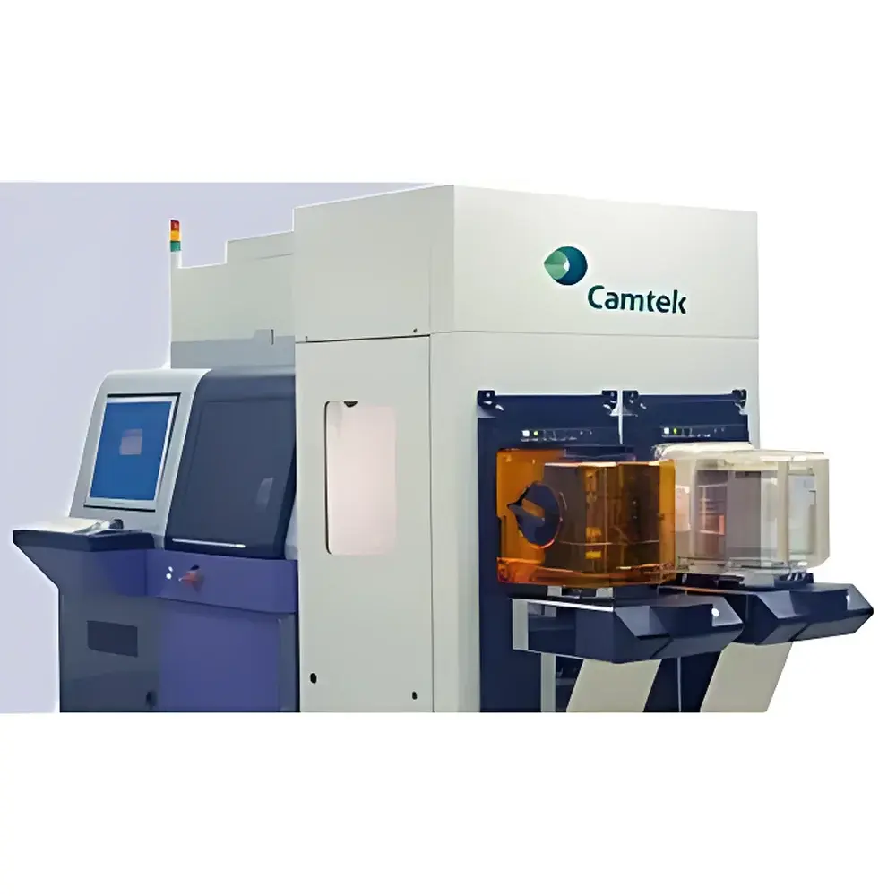
Camtek Falcon 800 Automated Optical Inspection System
| Brand | Camtek |
|---|---|
| Origin | Israel |
| Manufacturer Type | Authorized Distributor |
| Origin Category | Imported |
| Model | Falcon 800 |
| Pricing | Available Upon Request |
Overview
The Camtek Falcon 800 is an advanced automated optical inspection (AOI) and metrology platform engineered for high-precision 2D and 3D defect detection and geometric measurement in semiconductor front-end and advanced packaging processes. Built upon Camtek’s proprietary high-resolution imaging architecture and multi-spectral illumination technology, the system employs structured light projection, confocal chromatic sensing, and sub-pixel edge detection algorithms to deliver nanometer-level vertical resolution and micron-level lateral accuracy. It is specifically optimized for process-critical applications where dimensional fidelity and defect sensitivity are paramount — including stacked die packaging, 3D IC integration, System-in-Package (SiP), flip-chip interconnects, and fine-pitch wire bonding regions. The Falcon 800 supports both bare and framed wafers up to 300 mm in diameter, with configurable stage kinematics and vacuum chucking to ensure thermal and mechanical stability during high-speed scanning.
Key Features
- High-throughput AOI with integrated 3D topography mapping — enabling simultaneous defect classification and quantitative height/depth/width measurement
- Dual-mode imaging: Bright-field, dark-field, and oblique-angle illumination for enhanced contrast of surface anomalies, voids, bridging, and underfill delamination
- Automated focus-stacking and Z-height calibration using piezo-driven objective lens positioning for consistent repeatability across wafer fields
- Real-time defect review with hierarchical binning logic and customizable pass/fail thresholds aligned with IPC-A-610 and JEDEC J-STD-020 standards
- Modular hardware architecture supporting upgrade paths to inline integration via SECS/GEM protocol and factory automation interfaces (e.g., SMEMA, OHT)
- Robust environmental compensation: Active temperature drift correction and vibration isolation compliant with ISO 20484-2 for cleanroom Class 100 operation
Sample Compatibility & Compliance
The Falcon 800 accommodates silicon, compound semiconductor (GaAs, SiC), and advanced substrate wafers — including glass, ceramic, and organic laminate carriers used in fan-out wafer-level packaging (FOWLP) and panel-level processing. It accepts both unframed and framed wafers (standard frame sizes: 200 mm, 300 mm), with optional carrier handling modules for reticle trays and open cassettes. All measurement outputs comply with ISO/IEC 17025 traceability requirements when operated with certified reference standards. The system meets SEMI S2/S8 safety guidelines and supports audit-ready documentation for ISO 9001, IATF 16949, and FDA 21 CFR Part 11–compliant electronic records (with optional secure user authentication and full audit trail logging).
Software & Data Management
Powered by Camtek’s EAGLE™ software suite, the Falcon 800 provides a unified interface for recipe management, defect review, statistical process control (SPC), and cross-tool correlation. Measurement data is stored in a relational database (SQL-based) with support for ODBC export to MES or yield management platforms such as PDF Solutions Yield Explorer or Applied Materials Endura® Analytics. The software includes built-in GD&T evaluation tools per ASME Y14.5–2018, enabling direct reporting of flatness, coplanarity, bump height variation, and solder joint geometry. All software updates follow a formal change control process validated under GLP and GMP environments, with version history and configuration management logs retained for regulatory inspections.
Applications
- Post-bump inspection and height uniformity analysis for copper pillar and solder microbumps (pitch down to 40 µm)
- Die attach void detection and area quantification in chip-on-wafer and hybrid bonding processes
- Wire bond loop profile measurement — including bond heel height, sweep angle, and tail length deviation
- Underfill fillet geometry verification and capillary flow uniformity assessment
- Redistribution layer (RDL) line width/spacing metrology and planarity evaluation prior to lithography
- Final package inspection for lid warpage, mold compound surface defects, and cavity integrity in QFN, BGA, and WLCSP formats
FAQ
What wafer sizes does the Falcon 800 support?
The system handles 200 mm and 300 mm wafers, both framed and unframed, with optional adapters for non-standard carriers.
Does the Falcon 800 support automated defect classification (ADC)?
Yes — it integrates machine learning–assisted classification using supervised training on historical defect libraries, with configurable confidence thresholds and misclassification reporting.
Can the system be integrated into a 24/7 production line?
It supports continuous operation with dual-load port configuration, automated wafer ID reading (OCR + barcode), and predictive maintenance alerts via embedded sensor telemetry.
Is the Falcon 800 compliant with industry data security standards?
All data transmission uses TLS 1.2 encryption; local storage adheres to NIST SP 800-53 controls, and optional FIPS 140-2 cryptographic modules are available for government and defense applications.
How is measurement uncertainty characterized and validated?
Uncertainty budgets are generated per ISO/IEC Guide 98-3 (GUM) and verified annually using NIST-traceable step-height standards and pitch calibration masters supplied with each system.