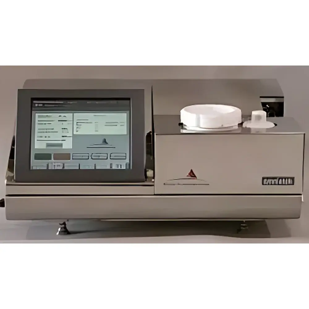
Nisene OmniEtch Wet Chemical Decapsulation System
| Brand | Nisene |
|---|---|
| Origin | USA |
| Manufacturer Type | Authorized Distributor |
| Product Category | Imported |
| Model | OmniEtch |
| Pricing | Available Upon Request |
Overview
The Nisene OmniEtch Wet Chemical Decapsulation System is a precision-engineered semiconductor failure analysis instrument designed for controlled, layer-selective removal of passivation, dielectric, and metallization layers from integrated circuits (ICs) and wafers. Unlike mechanical or plasma-based deprocessing methods, the OmniEtch employs a proprietary wet chemical etching principle—based on spatially confined, carrier-mediated reagent delivery—to achieve non-thermal, non-mechanical, and highly anisotropic material removal. The system utilizes a patented 36–6 carrier medium that encapsulates and delivers etchants through microchannels directly to targeted interfacial layers, enabling selective dissolution of metals (e.g., Al, Cu, TiN), polysilicon, and silicon dioxide without lateral undercutting or thermal damage. This mechanism ensures atomic-level planarity, eliminates beveling or rounding at feature edges, and preserves underlying structures for subsequent SEM, FIB, or EDX analysis—making it indispensable for root-cause analysis in high-reliability, automotive, aerospace, and advanced packaging applications.
Key Features
- Patented carrier-mediated wet etching technology enabling precise, layer-specific decapsulation with sub-micron vertical control
- User-configurable etchant chemistry selection—including HF-based, phosphoric-acid, and proprietary chelating formulations—for compatibility with Al, Cu, W, Co, SiO₂, SiN, and low-k dielectrics
- Programmable etch duration (1 s–24 h) and temperature control (20–80 °C) via integrated PID-regulated heating module
- Adjustable peristaltic pump speed (150–600 RPM) for dynamic flow-rate modulation and reagent residence time optimization
- Recirculating etchant path using the proprietary 36–6 carrier medium, reducing chemical consumption by up to 70% versus batch immersion
- Real-time process monitoring through fused quartz viewport (UV-transparent, 0.1 mm thickness) compatible with optical microscopy and in situ imaging
- Compact benchtop footprint (W×D×H: 450 × 520 × 380 mm) with IP54-rated enclosure for cleanroom-compatible operation (Class 1000 or better)
- Industrial-grade 7-inch color touchscreen HMI with intuitive graphical workflow interface, password-protected parameter locking, and audit-ready event logging
Sample Compatibility & Compliance
The OmniEtch supports decapsulation of packaged ICs (QFP, BGA, CSP, WLCSP, fan-out), bare dies, and full wafers up to 200 mm diameter. It accommodates leadframe, laminate, and ceramic substrates, as well as advanced packaging architectures including TSV, 2.5D/3D stacks, and heterogeneous integration assemblies. All wet chemistry protocols are developed in alignment with JEDEC J-STD-033, IPC-TM-650 2.6.25, and ASTM F2079 standards for semiconductor package deprocessing. The system’s firmware and data handling architecture comply with FDA 21 CFR Part 11 requirements for electronic records and signatures, supporting GLP/GMP environments through configurable user roles, electronic signature prompts, and immutable audit trails.
Software & Data Management
The OmniEtch Control Suite runs on a real-time Linux OS and provides full traceability across all operational cycles. Each run generates a timestamped, digitally signed .csv log containing etch parameters (temperature setpoint, actual reading, pump RPM, elapsed time), operator ID, sample ID, and chamber status flags. Logs are exportable via USB or network SMB share and integrate natively with LIMS platforms using standard OPC UA connectivity. Optional software modules include recipe versioning with rollback capability, automated report generation (PDF/HTML), and remote diagnostics via TLS-encrypted SSH tunnel—enabling secure off-site technical support without compromising network integrity.
Applications
- Failure isolation and defect localization in logic, memory, and power devices following electrical test failures
- Verification of metal layer integrity, via fill uniformity, and interlayer dielectric continuity in post-fab reliability stress testing
- Root-cause analysis of corrosion, electromigration, and TDDB-related failures in high-voltage and high-temperature applications
- Process validation and qualification of new packaging materials, underfill formulations, and wafer-level redistribution layers
- Forensic reverse engineering of security-critical ICs requiring intact gate-level topology preservation
- Support for ISO/IEC 17025-accredited laboratory workflows where metrological traceability and procedural repeatability are mandatory
FAQ
What types of etchants are compatible with the OmniEtch system?
The system supports aqueous and organic-phase etchants including buffered oxide etch (BOE), phosphoric acid mixtures, ammonium hydroxide–hydrogen peroxide solutions, and Nisene-certified proprietary formulations optimized for Cu barrier removal and low-k dielectric stability.
Can the OmniEtch process full 300 mm wafers?
No—the current configuration supports wafers up to 200 mm in diameter; 300 mm capability is available under custom engineering engagement with Nisene’s Applications Lab.
Is the quartz viewport suitable for in situ Raman or FTIR spectroscopy?
Yes—the fused quartz window transmits wavelengths from 190 nm to 2.5 µm, enabling integration with standard benchtop Raman spectrometers and mid-IR attenuated total reflectance (ATR) probes.
How does the system ensure reproducibility across different operators and shifts?
Through enforced recipe-based operation, hardware-enforced parameter limits, and electronic signature–gated execution—ensuring identical process conditions regardless of user identity or shift schedule.


