Copolymer Series Photoresist (MMA/MAA) by MicroChem
| Brand | MicroChem Corp |
|---|---|
| Origin | USA |
| Model | MMA(8.5)MAA |
| Solvent System | Ethyl Lactate |
| Viscosity Range | Adjustable via Concentration (Typical Spin-Coated Film Thickness: 50–500 nm) |
| Packaging Options | 500 mL, 1 L, 4 L, 20 L HDPE Bottles |
| Recommended Storage | 10–27 °C |
| Developer | MIBK:IPA (1:3 v/v) |
| Stripper | Remover PG |
| Diluent | A Thinner |
Overview
The Copolymer Series Photoresist (MMA/MAA) is a high-purity, solvent-based negative-tone resist engineered for advanced lithographic processes in semiconductor fabrication, MEMS development, and nanofabrication research. Composed of methyl methacrylate (MMA) copolymerized with 8.5 wt% methacrylic acid (MAA), this resist leverages the differential solubility of carboxylic acid-functionalized polymer chains in organic developer systems to achieve high-resolution pattern transfer. Its chemical design enables controlled dissolution inhibition and enhanced etch resistance when crosslinked—particularly under electron beam (e-beam) or deep ultraviolet (DUV) exposure. Unlike conventional PMMA resists, the MAA incorporation improves adhesion to silicon, SiO₂, and metal substrates while enabling tunable contrast and sensitivity across exposure doses (typically 100–500 µC/cm² for e-beam; 20–60 mJ/cm² for 365 nm i-line). The resist is formulated in ethyl lactate—a low-toxicity, high-boiling-point solvent compliant with industrial hygiene standards—to ensure batch-to-batch consistency and extended shelf life.
Key Features
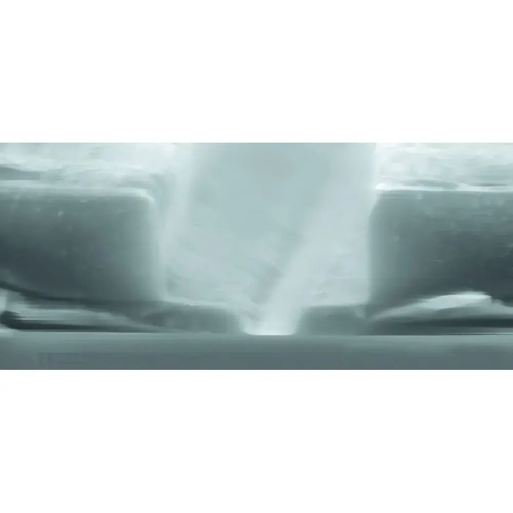
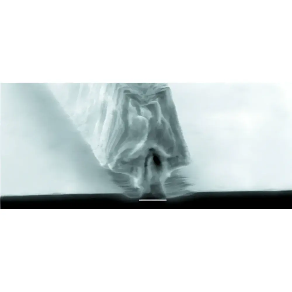
- Controlled acid content (8.5% MAA) optimized for dual-layer lift-off processes, enabling independent critical dimension (CD) control between top and bottom resist layers
- Compatible with both spin-coating (standard wafer processing) and dip-coating (for non-planar or large-area substrates)
- Adjustable film thickness (50–500 nm) via concentration modulation and spin speed (2,000–6,000 rpm), verified by ellipsometry and profilometry
- No added photoacid generators (PAGs) — suitable for direct-write e-beam lithography without post-exposure bake (PEB) requirements
- High thermal stability (Tg ≈ 105 °C) supports subsequent etch and deposition steps without flow or deformation
- Low metal ion contamination (<1 ppb Na, K, Fe, Cu), meeting SEMI F57 specifications for front-end-of-line (FEOL) applications
Sample Compatibility & Compliance
This resist demonstrates robust performance on silicon wafers (Si, SiO₂, SiN), III–V compounds (GaAs, InP), and metallic films (Al, Ti, Cr, Au). It adheres effectively after standard HMDS vapor priming or oxygen plasma surface activation. All lots undergo rigorous QC testing per MicroChem’s internal specification MCR-RES-004, including GPC molecular weight distribution (Mw/Mn ≤ 2.1), UV-Vis absorbance profiling (248 nm, 365 nm), and particulate count verification (<5 particles/mL ≥0.5 µm, ISO Class 5 cleanroom handling). The formulation complies with RoHS Directive 2011/65/EU and REACH Annex XVII restrictions. Safety data aligns with OSHA HCS 2012 and GHS classification (Skin Irrit. 2, Eye Irrit. 2, Aquatic Chronic 3).
Software & Data Management
While the Copolymer resist itself is a consumable material—not a hardware instrument—its process integration is supported by industry-standard lithography workflow tools. MicroChem provides downloadable process recipes for common platforms including EVG® Mask Aligners, Raith® e-line systems, and JEOL JBX-6300FS e-beam writers. Exposure dose calibration curves, spin-coating thickness vs. rpm charts, and developer time–temperature matrices are available in PDF and CSV formats through the MicroChem Technical Resource Portal. All documentation includes traceable lot-specific analytical reports (GPC, FTIR, residual solvent GC-MS), satisfying GLP audit requirements for R&D labs and qualified manufacturing environments operating under ISO 9001 and IATF 16949 frameworks.
Applications
- High-aspect-ratio nanostructure fabrication via e-beam lithography (e.g., plasmonic antennas, quantum dot arrays)
- Double-layer lift-off for sub-100 nm metal interconnect patterning (Ti/Au, Cr/Au stacks)
- Hard mask precursor for reactive ion etching (RIE) of Si, SiO₂, and SiN using CHF₃/O₂ or SF₆ chemistries
- Template-assisted electrodeposition of magnetic nanowires and nanotubes
- Maskless direct-write prototyping in university cleanrooms and pilot-line facilities
FAQ
What is the shelf life of Copolymer (8.5)MAA resist under recommended storage conditions?
Unopened bottles stored at 10–27 °C retain full performance for 12 months from date of manufacture. Once opened, use within 6 weeks under inert gas (N₂) purged environment to prevent moisture-induced aggregation.
Can this resist be used with UV contact lithography (i-line, g-line)?
Yes—though optimized for e-beam, it exhibits usable sensitivity under 365 nm (i-line) exposure at doses of 30–60 mJ/cm²; resolution is limited to ≥500 nm due to diffraction and scattering effects.
Is post-exposure bake (PEB) required?
No. As a non-chemically amplified resist, PEB is not necessary. However, a soft bake (90 °C, 90 s) is mandatory to remove residual solvent prior to exposure.
How does the MAA content affect development rate?
The 8.5% MAA level balances dissolution inhibition and developer selectivity: higher MAA increases polarity and developer solubility, but reduces etch resistance; lower MAA improves durability but compromises CD control in lift-off.
Are custom concentrations or packaging sizes available?
Yes—MicroChem offers OEM formulation services including viscosity-adjusted batches (cP range: 5–50 cP), nitrogen-flushed 100 mL ampoules for R&D, and bulk 200 L tote options for high-volume production lines.


