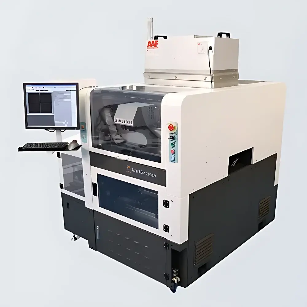
Capcon CAPCON-Die Bonder Automatic Die Bonder
| Brand | Capcon |
|---|---|
| Origin | Beijing, China |
| Manufacturer Type | Authorized Distributor |
| Regional Classification | Domestic (PRC) |
| Model | CAPCON-Die Bonder |
| Pricing | Available Upon Request |
Overview
The Capcon CAPCON-Die Bonder is a high-precision automatic die bonder engineered for semiconductor assembly and packaging applications. It operates on the principle of vision-guided pick-and-place with integrated thermal control and force-sensing feedback, enabling accurate die placement onto substrates such as leadframes, laminated PCBs, ceramic carriers, and silicon interposers. Designed for low-to-mid volume production and R&D prototyping, this system supports both epoxy-based and eutectic die attach processes. Its modular architecture accommodates optional upgrades including real-time bond-line thickness monitoring, nitrogen inerting, and pre-bond plasma cleaning—making it suitable for compound semiconductor, MEMS, and advanced packaging workflows where alignment tolerance, bond strength consistency, and process traceability are critical.
Key Features
- Vision-based alignment system with dual-camera optics (top-down and side-view), supporting sub-25 µm placement accuracy (3σ) under controlled environmental conditions
- Programmable bonding force range from 10 g to 500 g with closed-loop piezoelectric actuation and real-time load monitoring
- Heated bonding stage with temperature control from ambient to 300 °C (±1 °C stability), compatible with thermoset adhesives, silver sinter pastes, and Au–Si eutectic alloys
- Integrated XYZθ motion platform with linear motor drives and granite base for thermal and mechanical stability
- Tool-less nozzle and collet exchange system supporting multiple die sizes (50 µm to 25 mm) and carrier formats (gel packs, waffle trays, tape-and-reel)
- Compliant with SEMI S2/S8 safety standards; CE-marked with full electrical and functional safety documentation
Sample Compatibility & Compliance
The CAPCON-Die Bonder accommodates a broad spectrum of die geometries—including rectangular, square, and irregular shapes—with thicknesses ranging from 50 µm to 1.2 mm. It accepts standard industry carriers: JEDEC trays (including low-profile variants), EIA-481 tape-and-reel (8–44 mm widths), and custom vacuum chucks for fragile or warped substrates. Process compliance includes support for ISO 9001-certified manufacturing environments and compatibility with GLP/GMP documentation requirements via optional audit trail logging. While not FDA-registered as a medical device, its software architecture allows configuration to meet 21 CFR Part 11 electronic record and signature controls when deployed in regulated packaging lines.
Software & Data Management
The system runs on Capcon’s proprietary BondWare™ control software, built on a Windows 10 IoT Enterprise platform. It provides intuitive recipe management, step-by-step process scripting, and real-time parameter visualization (bond force vs. time, stage temperature ramp profiles, fiducial recognition confidence scores). All operational data—including placement coordinates, applied force curves, thermal soak durations, and machine status logs—are timestamped and exportable in CSV or XML format. Optional database integration enables direct linkage to MES platforms via OPC UA or SQL Server interfaces. Software updates are delivered through secure, authenticated channels with version-controlled release notes and validation reports per IEC 62304.
Applications
- Die attachment in power module assembly (IGBTs, SiC MOSFETs, GaN HEMTs)
- R&D-scale flip-chip and hybrid bonding development requiring precise die registration
- MEMS sensor packaging involving fragile dies and anisotropic conductive films (ACF)
- LED and micro-LED transfer printing for display substrate integration
- Advanced heterogeneous integration trials, including chiplets on organic substrates and glass interposers
- Qualification testing of new die attach materials under controlled thermal-mechanical stress profiles
FAQ
What types of die attach materials are supported by the CAPCON-Die Bonder?
It supports conductive epoxies, non-conductive pastes (NCP), silver sinter materials, solder preforms, and eutectic alloys (e.g., Au–Si, Au–Sn), provided appropriate thermal profiles and dispensing hardware are configured.
Does the system include fiducial recognition capability for warped or non-planar substrates?
Yes—its dual-vision system performs multi-point fiducial detection and applies real-time Z-height compensation using laser displacement sensors integrated into the bond head.
Can the CAPCON-Die Bonder be integrated into an existing cleanroom automation line?
It features SECS/GEM protocol support and standard SMEMA handshaking interfaces, enabling seamless integration with conveyor-based material handling systems and factory host controllers.
Is remote diagnostics and service support available outside mainland China?
Capcon provides remote access via encrypted VNC sessions for firmware troubleshooting and calibration verification; on-site engineering support is coordinated through regional authorized service partners in APAC, EMEA, and North America.
Related Products


