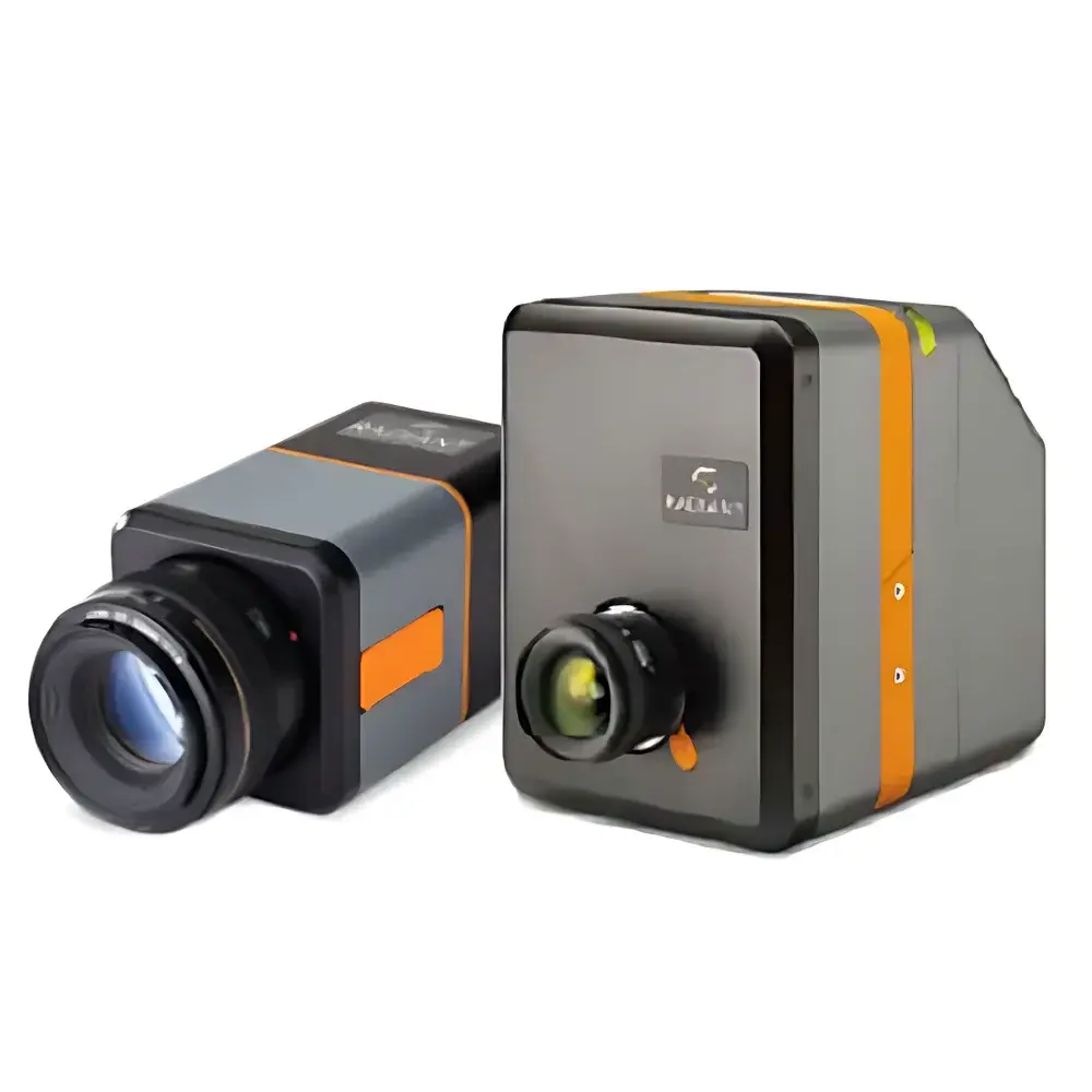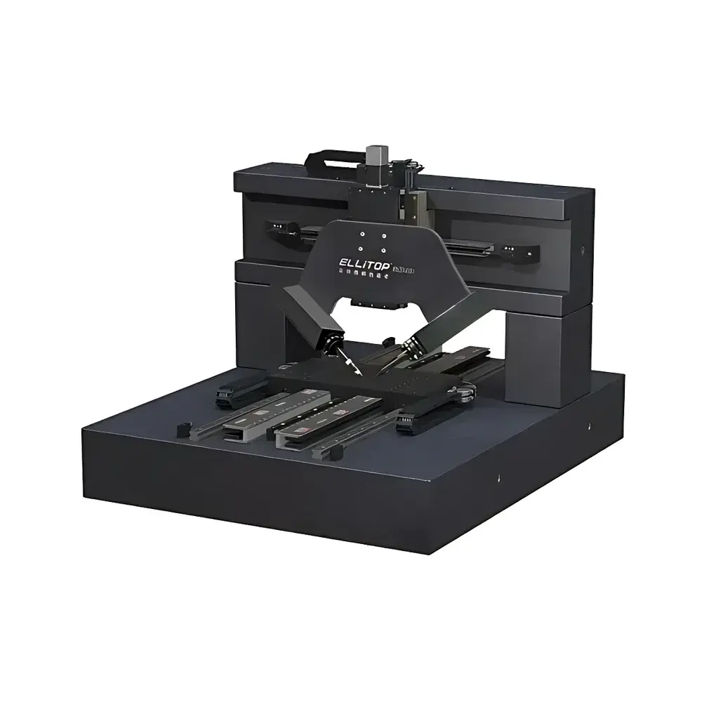
ELLITOP EP800 Spectroscopic Ellipsometer System
| Brand | ELLITOP |
|---|---|
| Origin | Beijing, China |
| Model | EP800 |
| Spectral Range | 245–1000 nm (customizable) |
| Incident Angles | 60° or 65° (selectable) |
| Measurement Repeatability | 0.01 nm |
Overview
The ELLITOP EP800 Spectroscopic Ellipsometer System is a purpose-built optical metrology platform engineered for high-precision, non-destructive characterization of thin-film structures in flat-panel display (FPD) manufacturing. Based on the physical principle of spectroscopic ellipsometry—measuring the change in polarization state of reflected light across a broad wavelength range—the EP800 quantifies amplitude ratio (Ψ) and phase difference (Δ) to extract critical nanoscale film parameters. Unlike interferometric or reflectometric methods, ellipsometry provides intrinsic sensitivity to sub-nanometer thickness variations and decouples optical constants (n, k) from geometric thickness, enabling robust modeling of complex multilayer stacks (e.g., ITO/SiNx/organic emissive layers on glass or flexible substrates). The system operates at fixed incident angles (60° or 65°), optimized for high signal-to-noise ratio in production-relevant spectral windows (245–1000 nm), supporting both UV-VIS-NIR analysis and material dispersion modeling.
Key Features
- Non-contact, non-destructive measurement: Eliminates risk of surface damage or contamination during inline or offline inspection.
- High spatial resolution mapping: Motorized XY stage enables automated multi-point scanning across large-area substrates (up to Gen 8.5 glass panels with optional stage extension).
- Sub-second per-point acquisition: Full-spectrum Ψ/Δ data collection completed in ≤3 seconds per location, facilitating high-throughput process monitoring.
- Atomic-layer sensitivity: Repeatability of ±0.01 nm enables detection of monolayer-level thickness drifts—critical for controlling sputtered metal oxides or evaporated organic layers.
- One-click workflow automation: Integrated measurement sequence includes auto-alignment, background correction, model fitting, and report generation without manual intervention.
- Factory integration readiness: Equipped with SECS/GEM-compliant communication protocols (RS-232, TCP/IP, Modbus) and mechanical/electrical interfaces for seamless integration into vacuum coater lines or cleanroom AOI stations.
Sample Compatibility & Compliance
The EP800 supports rigid (glass, quartz, silicon wafers) and flexible (PI, PET, PEN) substrates up to 300 mm × 300 mm. Its optical design accommodates transparent, semi-transparent, and opaque base materials—including patterned TFT arrays—via adjustable beam spot size (100–500 µm diameter) and variable focus optics. All measurement routines adhere to ISO 15630-3 (reinforcing steel testing), ASTM F1997 (ellipsometry terminology), and JIS K 7105 (optical properties of plastics), with traceability to NIST-traceable calibration standards. For regulated environments, audit trail logging, user access control, and electronic signature support comply with FDA 21 CFR Part 11 requirements when deployed with validated software configurations.
Software & Data Management
The proprietary ELLITOP Analysis Suite v4.2 provides full modeling capability using Cauchy, Tauc-Lorentz, Cody-Lorentz, and B-Spline dispersion models. Users define multilayer stack architectures via intuitive layer-tree interface, assign optical models per layer, and perform global regression with Levenberg-Marquardt optimization. Raw Ψ/Δ spectra, fitted curves, confidence intervals, and covariance matrices are exportable in CSV, XML, and HDF5 formats. Database integration (ODBC-compliant) allows direct linkage to MES systems for SPC charting (X-bar R, Cpk) and real-time yield analytics. Software validation documentation (IQ/OQ/PQ templates) and change control logs are included for GMP/GLP-regulated facilities.
Applications
- Thickness and optical constant monitoring of transparent conductive oxides (ITO, AZO, IGZO) in OLED and LCD array fabrication.
- In-process verification of anti-reflection (AR), hard-coat, and barrier layers on cover glass and touch sensors.
- Characterization of photoresist development uniformity and etch selectivity in photolithography processes.
- Quality assurance of encapsulation layers (Al₂O₃, SiNₓ) deposited by ALD or PECVD for flexible OLED encapsulation.
- R&D support for novel 2D materials (MoS₂, graphene oxide) and perovskite thin films used in next-generation displays and photovoltaics.
FAQ
What is the minimum measurable film thickness with the EP800?
The system reliably resolves films as thin as 0.3 nm on optically smooth substrates, limited primarily by surface roughness and ambient noise—not instrument resolution.
Can the EP800 measure on patterned or textured surfaces?
Yes—using spot-size optimization and angular averaging algorithms, it characterizes average film properties over micro-patterned regions (e.g., pixel wells) with <5% uncertainty relative to planar references.
Is spectral range customization available beyond 245–1000 nm?
Extended ranges (e.g., 190–1700 nm) are supported via optional grating and detector modules; lead time and calibration validation apply.
Does the system support real-time feedback to deposition tools?
Yes—through programmable digital I/O and Ethernet-based recipe triggers, the EP800 can send endpoint signals or thickness deviation alerts to PLCs or chamber controllers.
How is measurement uncertainty quantified and validated?
Uncertainty budgets follow GUM (JCGM 100:2018) methodology, incorporating contributions from spectral calibration, angle encoder drift, polarization element retardance error, and model parameter correlation—fully documented in the supplied uncertainty report.