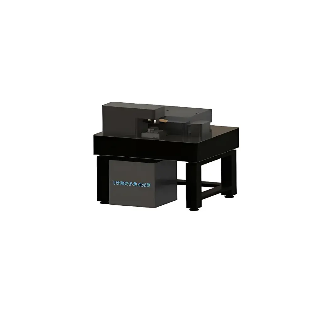
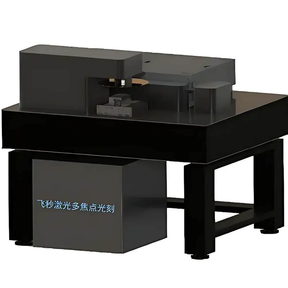
FP NanoPrinter Femtosecond Multi-Focal Holographic Lithography System
| Brand | Other brands |
|---|---|
| Origin | Hong Kong |
| Manufacturer Type | General distributor |
| Domestic/Imported | Domestic |
| Model | FP NanoPrinter |
| Price Range | USD 140,000 – 700,000 |
| Key Features | DMD-based dynamic holographic patterning |
| Laser Safety Class | Class 4 |
| XY/Z Feature Size | 142 nm / 175 nm |
| Resolution (Diffraction-Limited) | 285 nm / 500 nm |
| Layer Spacing | ≥ 0.05 µm |
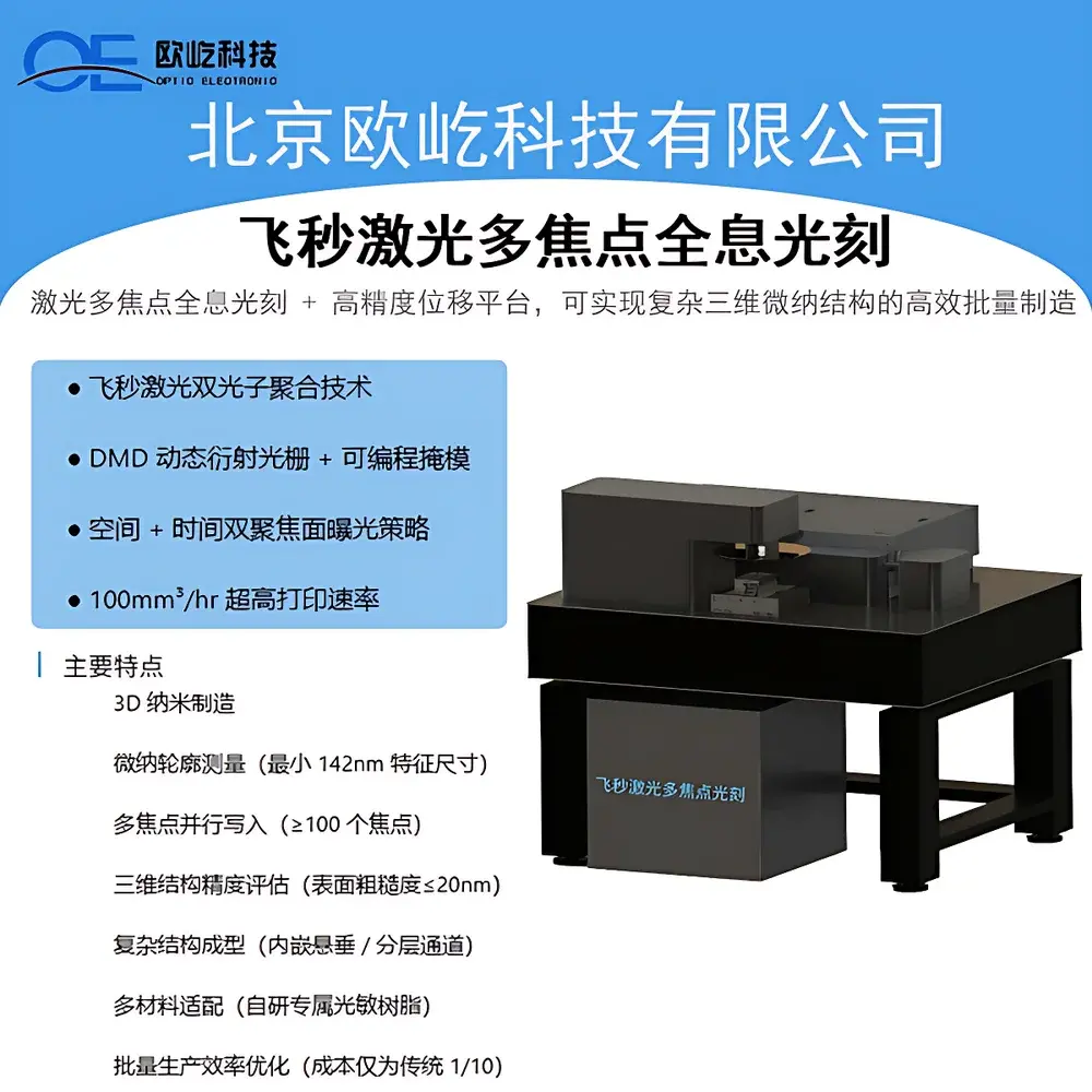
| Throughput | 100 mm³/hr |
| Parallel Foci | ≥ 100 |
| Surface Roughness | ≤ 20 nm |
| Operating Temp | 23 ± 1 ℃ |
| RH | < 50% (recommended < 35%) |
| Vibration Requirement | Active isolation required |
| Power Supply | 220 V, > 35 A |
Overview
The FP NanoPrinter is a turnkey femtosecond multi-focal holographic lithography system engineered for high-throughput, sub-150 nm resolution 3D nanofabrication. Unlike conventional point-scanning two-photon polymerization (TPP) systems, the FP NanoPrinter employs a spatially and temporally modulated femtosecond light sheet generated via a digital micromirror device (DMD) operating simultaneously as a programmable diffractive optical element and dynamic mask. This architecture enables true parallel volumetric exposure—projecting hundreds of independently addressable foci into photosensitive resins in a single exposure cycle. The system leverages nonlinear absorption physics under tightly confined, ultrashort laser pulses to achieve voxel confinement below the diffraction limit, with axial and lateral resolution validated at 175 nm and 142 nm respectively under optimized conditions. Its core measurement and fabrication principle rests on holographic beam shaping combined with precision synchronized stage translation, delivering deterministic 3D microstructure synthesis without mechanical scanning latency. Designed for semiconductor process development labs, photonics R&D centers, and advanced packaging facilities, the FP NanoPrinter bridges the gap between research-grade nanofabrication and scalable prototyping—supporting overlay-critical applications such as nano-optical elements, photonic crystals, microfluidic interconnects, and MEMS-compatible structural templates.
Key Features
- DMD-driven holographic illumination enabling real-time, arbitrary multi-focus pattern generation with per-focus intensity and phase control
- Femtosecond light-sheet projection with sub-micron depth confinement and minimal thermal diffusion, ensuring high-fidelity 3D voxel placement
- Integrated high-precision air-bearing XYZ stage with <10 nm repeatability and synchronized motion control for seamless layer stacking
- Parallel writing capability supporting ≥100 simultaneous foci, reducing exposure time by up to two orders of magnitude versus serial TPP
- Native support for overhangs, nested channels, and topologically complex geometries without sacrificial scaffolding or post-processing
- Class 4 laser subsystem compliant with IEC 60825-1:2014 and ANSI Z136.1–2022 safety standards, including interlocked enclosure and beam path containment
- Thermally stabilized optical bench and environmental monitoring suite (temperature, humidity, particulate, vibration) for GLP-aligned operation
Sample Compatibility & Compliance
The FP NanoPrinter is compatible with a broad range of commercially available and custom-formulated photoresists—including IP-L 780, SZ2080, OrmoComp®, and hybrid organic-inorganic sol-gels—enabling multi-material integration within a single print run. Substrate options span silicon wafers (up to 200 mm), fused silica, sapphire, and flexible polymer films. All hardware and firmware comply with CE marking requirements for machinery (2006/42/EC) and electromagnetic compatibility (2014/30/EU). Data integrity protocols align with FDA 21 CFR Part 11 expectations for electronic records and signatures, including audit trail logging, user access controls, and immutable parameter archiving. The system supports ISO 9001-certified calibration workflows and is routinely deployed in cleanroom environments meeting ISO Class 7 (Class 10,000) particle specifications.
Software & Data Management
AstraWrite—a dedicated GUI platform—provides end-to-end workflow management from STL/BMP import to exposure sequence generation and real-time process monitoring. It includes built-in optical simulation tools for predicting voxel overlap, dose distribution, and refractive index modulation based on material dispersion models. All print jobs are timestamped and digitally signed; raw exposure logs, stage trajectories, and laser power telemetry are stored in HDF5 format with metadata tagging per ISO/IEC 11179. Export options include standardized G-code derivatives for cross-platform toolchain integration and JSON-based recipe exchange for multi-system fleet management. Remote diagnostics and firmware updates are performed over TLS-encrypted Ethernet connections, with optional integration into enterprise LIMS via RESTful API.
Applications
- Semiconductor: Fabrication of alignment marks, overlay metrology targets, and test structures for EUV and DUV lithography process validation
- Optics & Photonics: Rapid prototyping of freeform microlens arrays, polarization-selective metasurfaces, and integrated waveguide couplers
- Biomedical Devices: Production of scaffold-free tissue engineering matrices, microfluidic organ-on-chip interfaces, and implantable biosensor housings
- Microelectromechanical Systems (MEMS): Direct-write fabrication of compliant mechanisms, resonant cantilevers, and inertial sensor proof masses
- Advanced Packaging: Creation of redistribution layer (RDL) alignment fiducials, underfill void mitigation structures, and thermal interface microstructures
FAQ
What is the minimum printable feature size achievable with the FP NanoPrinter?
The system achieves a verified feature size of 142 nm (XY) and 175 nm (Z) under standard operating conditions using high-NA oil-immersion objectives and optimized resist chemistry.
Does the system support automated focus correction during printing?
Yes—integrated interferometric focus sensing and closed-loop Z-stage feedback enable real-time focal plane stabilization across temperature drifts and substrate warpage.
Can the FP NanoPrinter be integrated into a Class 100 (ISO 5) cleanroom environment?
The base configuration meets ISO Class 7; optional upgrades—including HEPA-filtered internal air circulation and stainless-steel vacuum-compatible enclosures—are available for ISO 5 deployment.
Is remote operation supported for multi-site R&D collaboration?
Full remote desktop access, secure job queuing, and collaborative annotation tools are enabled via the AstraWrite cloud gateway with role-based permissions.
What documentation is provided for regulatory submission in medical device manufacturing?
Comprehensive Design History File (DHF) excerpts, Risk Management File (ISO 14971), and Verification & Validation test reports are supplied upon request for FDA 510(k) or CE MDR pathways.


