Al2O3 Crystal Substrates – Hefei Kejing Sapphire Wafers (C-, A-, M-, R-Plane)
| Kejing Al2O3 Crystal Substrates | Brand: Hefei Kejing |
|---|---|
| Origin | Anhui, China |
| Manufacturer Type | Authorized Distributor |
| Origin Category | Domestic |
| Model | Al2O3 Crystal Substrates |
| Pricing | Available Upon Request |
| Crystal Structure | Hexagonal (α-Al₂O₃) |
| Lattice Parameters | a = 4.758 Å, c = 12.992 Å |
| Orientations | C-plane (0001), A-plane (11̄20), M-plane (10̄10), R-plane (11̄02) |
| Purity | >99.99% |
| Melting Point | 2040 °C |
| Density | 3.98 g/cm³ |
| Mohs Hardness | 9 |
| Thermal Expansion Coefficient | 7.5 × 10⁻⁶ /°C |
| Specific Heat Capacity | 0.10 cal/(g·°C) |
| Thermal Conductivity | 46.06 W/(m·K) @ 0 °C, 25.12 W/(m·K) @ 100 °C, 12.56 W/(m·K) @ 400 °C |
| Dielectric Constant | ε∥a ≈ 9.4, ε∥c ≈ 11.58 @ 300 K |
| Loss Tangent | tanδ < 2×10⁻⁵ (∥a), <5×10⁻⁵ (∥c) |
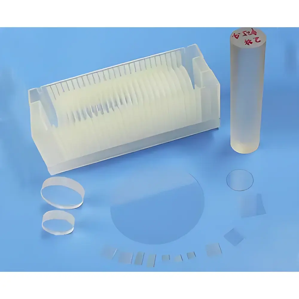
| Surface Finish | Single- or Double-Side Polished, Ra < 0.5 nm |
| Dimensional Tolerances | Orientation ±0.5°, Thickness ±0.01 mm |
| Standard Sizes | Ø2" × 0.5 mm, Ø3" × 0.5 mm, 10 × 10 × 0.5 mm, 10 × 5 × 0.5 mm |
| Packaging | Class 1000 Cleanroom Assembly, Class 100 Clean Bag or Individual Cassette |
Overview
Al2O3 crystal substrates—commonly known as sapphire wafers—are single-crystal α-alumina plates grown via the Verneuil or Kyropoulos method and precision-oriented along defined crystallographic planes. As a wide-bandgap (9.3 eV) insulator with exceptional thermal, mechanical, and chemical stability, sapphire serves as a foundational platform for epitaxial growth of III–V and III–nitride semiconductors—including GaN, AlN, and InGaN—enabling high-efficiency blue, green, and white light-emitting diodes (LEDs), laser diodes (LDs), and high-power RF devices. Its transparency from deep UV (~150 nm) to mid-infrared (~5.5 µm), combined with negligible absorption in the visible spectrum and low dielectric loss, makes it indispensable for optical windows, sensors, and MEMS resonators operating under extreme thermal or corrosive conditions.
Key Features
- High-purity α-Al2O3 monocrystals (>99.99% trace-metal-free), grown under controlled oxidizing atmosphere to minimize oxygen vacancy defects
- Precise orientation control across four standard crystallographic planes: C-plane (0001), A-plane (11̄20), M-plane (10̄10), and R-plane (11̄02), each offering distinct surface energy, step-terrace structure, and lattice-matching characteristics for heteroepitaxy
- Ultra-smooth surface finish: single- or double-side polished wafers with RMS roughness <0.5 nm (Ra < 5 Å), verified by atomic force microscopy (AFM) and optical interferometry
- Dimensional tolerances maintained at ±0.5° angular deviation from nominal orientation and ±0.01 mm thickness uniformity, critical for repeatable thin-film nucleation and stress management
- Thermally robust architecture: stable up to 2040 °C in air; coefficient of thermal expansion closely matched to GaN (≈5.6 × 10⁻⁶ /°C) on C-plane, reducing interfacial strain during MOCVD or MBE growth
- Class 1000 cleanroom processing and Class 100 cleanbag or individual cassette packaging ensure particulate contamination <10 particles ≥0.5 µm per wafer surface
Sample Compatibility & Compliance
These substrates are routinely qualified for use in ISO/IEC 17025-accredited thin-film deposition facilities and comply with industry-standard handling protocols for semiconductor-grade materials. While not certified to ISO 9001 or IATF 16949 at the distributor level, all wafers undergo full lot traceability documentation—including X-ray diffraction (XRD) rocking curve FWHM data, surface inspection reports, and orientation verification certificates—supporting GLP-compliant process validation. They meet ASTM F797-22 requirements for sapphire substrate dimensional specifications and are compatible with standard photolithography, etching, and metallization processes used in compound semiconductor fabrication lines.
Software & Data Management
As passive crystalline substrates, Al2O3 wafers do not incorporate embedded firmware or require proprietary software. However, their metrological data—including orientation angle deviation, surface flatness (TTV, BOW, Warp), and spectral transmission profiles—is provided in standardized ASCII or CSV format upon request. This enables seamless integration into automated fab material tracking systems (e.g., MES platforms compliant with SEMI E10/E142 standards) and supports statistical process control (SPC) analysis for yield optimization in LED and power electronics manufacturing.
Applications
- Heteroepitaxial growth of GaN-based LEDs and LDs for solid-state lighting and optical data storage
- Template layers for AlN and ScAlN piezoelectric films in high-frequency SAW/BAW filters
- Substrate for high-temperature microelectromechanical systems (HT-MEMS) and harsh-environment pressure sensors
- Infrared-transmissive windows in spectroscopic instrumentation (FTIR, QCL-based gas analyzers)
- Dielectric carrier substrates for GaAs and InP-based microwave monolithic integrated circuits (MMICs)
- Base material for ion implantation masking layers and radiation-hardened device prototyping
FAQ
What crystal orientations are available, and how do they differ in epitaxial performance?
C-plane (0001) offers highest symmetry and is dominant for GaN-on-sapphire LEDs; A- and R-planes enable nonpolar growth to reduce quantum-confined Stark effects; M-plane allows semi-polar orientation for improved internal quantum efficiency.
Can custom orientations or off-cut angles be supplied?
Yes—orientations within ±2° of any rational hkl plane and off-cuts from 0.1° to 4.0° are available upon technical review and minimum order quantity agreement.
Are these substrates suitable for direct metal deposition without adhesion layers?
Titanium, nickel, and chromium adhere well to native sapphire surfaces after oxygen plasma pretreatment; however, a Ti or NiCr adhesion layer is recommended for Au, Cu, or Al metallization requiring long-term thermal cycling reliability.
Do you provide surface analysis reports with each shipment?
Standard certification includes XRD pole figure, AFM roughness map, and optical microscopy images; full QC dossier (including SEM cross-section, EDX, and ellipsometry) is available as an add-on service.
What is the typical lead time for custom dimensions or polishing specifications?
Standard stock sizes ship within 5 business days; custom orders—including nonstandard thicknesses, edge profiles (rounded or chamfered), or epi-ready surface treatments—require 3–6 weeks depending on batch scheduling and metrology queue.
Related Products


 and Vehicle Classification System")