Ge Crystal Substrates (High-Purity Germanium Wafers for QCM and Semiconductor Applications)
| Brand | Hefei Kejing |
|---|---|
| Origin | Anhui, China |
| Manufacturer Type | Authorized Distributor |
| Origin Category | Domestic |
| Model | Ge Crystal Substrates |
| Pricing | Available Upon Request |
| Density | 5.765 g/cm³ |
| Melting Point | 937.4 °C |
| Thermal Conductivity | 64 W/(m·K) |
| Doping Options | Undoped / Sb-doped / In- or Ga-doped |
| Conductivity Type | Intrinsic / n-type / p-type |
| Resistivity | >35 Ω·cm (intrinsic) / 0.05 Ω·cm (Sb-doped) / 0.05–0.1 Ω·cm (In/Ga-doped) |
| Etch Pit Density (EPD) | < 4×10³ cm⁻² for all dopant types |
| Standard Orientations | <111>, <100>, <110> ± 0.5° |
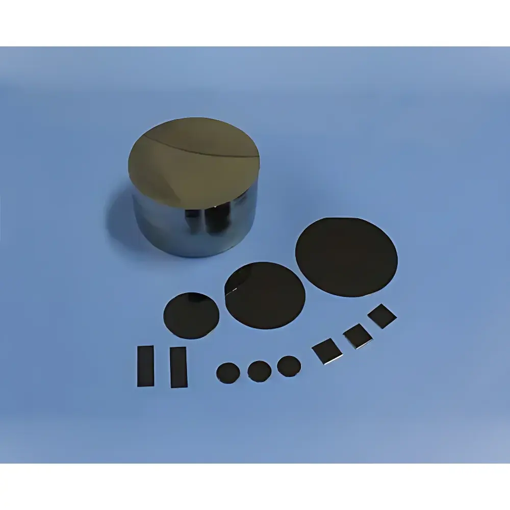
| Standard Polished Wafer Sizes | Ø25.4 mm × 0.3 mm, Ø50.8 mm × 0.5 mm |
| Surface Roughness (Ra) | < 0.5 nm (<110>, non-chemically polished) |
| Packaging | Individual 100-class clean bags in Class 1000 cleanroom environment |
Overview
Ge Crystal Substrates are high-purity, single-crystal germanium wafers engineered for precision applications in quartz crystal microbalance (QCM) sensor development, infrared (IR) optical component fabrication, semiconductor device prototyping, and photovoltaic research. Germanium’s unique combination of high refractive index (n ≈ 4.0 in mid-IR), low absorption in the 2–14 µm spectral range, and excellent lattice match with III–V compound semiconductors makes it an indispensable substrate material for epitaxial growth and surface-sensitive gravimetric sensing. These substrates are grown via the Czochralski (CZ) method under ultra-high vacuum conditions, followed by precision orientation verification using X-ray diffraction (XRD), double-side lapping, mechanical polishing, and final chemical-mechanical planarization (CMP) to achieve atomic-level flatness and low defect density.
Key Features
- Ultra-low etch pit density (EPD < 4×10³ cm⁻²) across all doping variants—ensuring minimal surface nucleation sites for thin-film deposition and reliable QCM frequency stability.
- Controlled dopant incorporation (Sb, In, Ga) enabling tunable carrier concentration and conductivity type (n-type or p-type), critical for integrated electrochemical transducer design and heterostructure compatibility studies.
- Precision crystallographic orientation tolerance (±0.5°) for , , and planes—supporting reproducible epitaxial alignment in MBE and MOCVD systems, as well as anisotropic etching behavior in microfabrication workflows.
- Surface roughness (Ra) < 0.5 nm on -oriented polished wafers—meeting stringent requirements for molecular adsorption studies and high-Q resonator fabrication where interfacial energy dissipation must be minimized.
- Class 1000 cleanroom processing and Class 100 cleanbag packaging—reducing organic and particulate contamination to levels compatible with ISO 14644-1 Class 5 environments during device integration.
Sample Compatibility & Compliance
These Ge substrates are fully compatible with standard QCM electrode sputtering (e.g., Au, Pt, Cr/Au bilayers), ALD precursors (e.g., TiN, Al₂O₃), and solution-based functionalization chemistries (e.g., silanization, thiol self-assembled monolayers). They conform to ASTM F1531–22 for semiconductor wafer flatness specifications and meet ISO/IEC 17025 traceability requirements for dimensional metrology when measured using calibrated interferometric profilometry. While not certified to USP or FDA 21 CFR Part 11 out-of-the-box, the documented lot-specific EPD, resistivity, and orientation data support GLP-compliant experimental recordkeeping in regulated R&D environments.
Software & Data Management
No embedded firmware or proprietary software is associated with the substrate itself; however, each shipment includes a Certificate of Conformance (CoC) listing batch-specific parameters—including XRD rocking curve full-width at half-maximum (FWHM), four-point probe resistivity maps, and surface inspection reports (per SEM/AFM validation on sample wafers). Digital CoCs are provided in PDF/A-1b format, supporting long-term archival per ISO 14721 (OAIS) standards. Integration with laboratory information management systems (LIMS) is enabled via standardized CSV metadata export containing wafer ID, orientation, doping, thickness, and EPD values.
Applications
- Quartz crystal microbalance (QCM) platforms requiring IR-transparent, high-acoustic-impedance substrates for real-time monitoring of polymer film swelling, biomolecular binding kinetics, and gas-phase adsorption in harsh thermal environments.
- Heteroepitaxial growth of PbTe, CdTe, and HgCdTe layers for uncooled IR focal plane arrays—leveraging Ge’s near-lattice-match (≈0.4% mismatch) and thermal expansion coefficient compatibility (5.8×10⁻⁶ K⁻¹).
- Reference substrates in X-ray reflectometry (XRR) and grazing-incidence small-angle X-ray scattering (GISAXS) calibration protocols due to its high electron density and isotropic scattering cross-section.
- Solar cell back-surface field (BSF) layers and tandem cell bottom junctions—particularly in III–V/Ge multijunction architectures targeting >30% AM1.5G conversion efficiency.
- Electrochemical impedance spectroscopy (EIS) studies involving redox-active interfaces, where controlled bulk conductivity enables decoupling of charge-transfer resistance from solution-phase diffusion limitations.
FAQ
Are these Ge substrates suitable for direct use in commercial QCM instruments?
Yes—standard Ø25.4 mm and Ø50.8 mm diameters match common AT-cut quartz holder geometries; thicknesses (0.3 mm and 0.5 mm) ensure mechanical rigidity while maintaining optimal shear-mode coupling efficiency.
Can custom orientations beyond // be supplied?
Yes—custom cuts such as , , or off-axis wafers are available upon request, subject to minimum order quantity and extended lead time for orientation verification and polishing optimization.
Is resistivity uniformity across the wafer surface guaranteed?
Resistivity mapping is performed on representative samples per batch; typical radial variation is ≤±5% for doped variants and ≤±10% for intrinsic Ge—fully documented in the CoC.
Do you provide surface termination certificates (e.g., oxide thickness, carbon contamination)?
Standard delivery includes native GeO₂ layer characterization via XPS (depth ~1.2 nm); additional surface analysis (TOF-SIMS, ellipsometry) can be arranged as an add-on service with NDA-compliant reporting.
Related Products

")