Silicon (Si) Crystal Substrates for Quartz Crystal Microbalance (QCM) and Electrochemical Applications
| Brand | Hefei Kejing |
|---|---|
| Origin | Anhui, China |
| Manufacturer Type | Authorized Distributor |
| Origin Category | Domestic (PRC) |
| Model | Si Crystal Substrate |
| Pricing | Upon Request |
| Doping Type | B- or P-doped (p-type) / N-doped (n-type) |
| Resistivity | 10⁻³ – 40 Ω·cm |
| EPD (Etch Pit Density) | ≤100 cm⁻² |
| Oxygen Content | ≤1.8 × 10¹⁸ cm⁻³ |
| Carbon Content | ≤5 × 10¹⁶ cm⁻³ |
| Crystal Orientation | <100>, <110>, or <111> ± 0.5° (custom orientations available) |
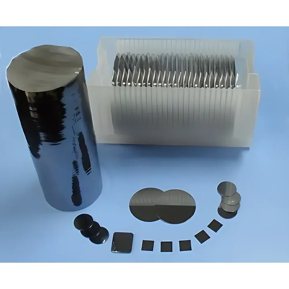
| Standard Dimensions | Ø25.4 mm × 0.30 mm, Ø50.8 mm × 0.50 mm, Ø76.2 mm × 0.50 mm, Ø101.6 mm × 0.60 mm |
| Surface Roughness | Ra < 0.1 nm (10 Å) |
| Optional Surface Modifications | Thermal SiO₂ layer (thickness customizable), or pre-fabricated multilayer stacks: Si/SiO₂/Ti/Pt |
| Packaging | Individual wafers in Class 100 cleanroom bags |
Overview
Silicon (Si) crystal substrates serve as high-purity, structurally defined mechanical and electronic foundations for advanced electrochemical sensing platforms—particularly Quartz Crystal Microbalance (QCM) systems requiring rigid, low-dissipation support structures for resonator electrode deposition and interfacial mass monitoring. Unlike conventional quartz blanks, Si substrates offer superior thermal conductivity, tunable electronic properties via controlled doping, and compatibility with standard semiconductor processing techniques—including photolithography, sputtering, and atomic layer deposition. These wafers are grown via the Czochralski (CZ) method under ultra-high-purity inert atmosphere, followed by double-side chemical-mechanical polishing (CMP) to achieve atomic-level flatness and minimal surface defect density. Their use extends beyond QCM transducers to reference electrodes in potentiostatic cells, working electrode supports in corrosion studies, and base layers for functionalized thin-film sensors in gas-phase or liquid-phase electrochemical impedance spectroscopy (EIS).
Key Features
- High crystalline integrity with etch pit density (EPD) ≤100 cm⁻², ensuring minimal dislocation-induced signal noise in resonant frequency measurements.
- Controlled dopant profile (boron or phosphorus) enabling precise resistivity tuning from 10⁻³ to 40 Ω·cm—critical for minimizing parasitic current paths in multi-electrode QCM-D configurations.
- Ultra-low interstitial oxygen (≤1.8 × 10¹⁸ cm⁻³) and substitutional carbon (≤5 × 10¹⁶ cm⁻³) concentrations, reducing dielectric loss and enhancing long-term stability under humid or oxidizing environments.
- Crystallographic orientation options (, , ± 0.5°) allow optimization of surface energy, step-edge density, and epitaxial growth behavior for subsequent metal or oxide film deposition.
- Surface roughness Ra < 0.1 nm (10 Å) measured by AFM over 5 × 5 µm² areas—essential for uniform thin-film adhesion and reproducible Sauerbrey mass calibration.
- Available with thermally grown SiO₂ layers (10–500 nm thickness, dry/wet oxidation variants) or integrated metallization stacks (Si/SiO₂/Ti/Pt) fabricated under ISO Class 5 cleanroom conditions and documented per ISO 14644-1.
Sample Compatibility & Compliance
These silicon substrates are compatible with standard QCM sensor holders (e.g., Inficon, Stanford Research Systems, and custom vacuum-compatible flanges) and electrochemical flow cells requiring planar, non-porous supports. All wafers undergo full spectral ellipsometry, four-point probe resistivity mapping, and X-ray diffraction (XRD) rocking curve analysis prior to release. Certificate of Analysis includes traceable metrology data aligned with ASTM F1563 (Standard Specification for Silicon Wafers for Epitaxial Use) and SEMI MF1530 (Test Method for Resistivity of Silicon Wafers). Packaging complies with SEMI E10 (Specification for Cleanroom Packaging of Semiconductor Wafers) and is suitable for GLP-compliant laboratories operating under ISO/IEC 17025 accreditation requirements.
Software & Data Management
While the substrate itself is a passive component, its specifications directly impact data fidelity in time-resolved QCM experiments. When integrated into automated QCM systems (e.g., Q-Sense E4, Biolin Scientific), these Si wafers enable stable baseline drift < 0.5 Hz/h over 24 h under controlled temperature (±0.02 °C) and humidity (±1% RH) conditions—supporting reliable quantification of sub-monolayer adsorption kinetics. Raw frequency and dissipation shifts are traceable to NIST-traceable calibration standards when used with instruments compliant with FDA 21 CFR Part 11 for audit trail generation and electronic signature validation.
Applications
- QCM-D sensor platforms for real-time monitoring of protein adsorption, polymer brush swelling, and lipid bilayer formation in aqueous electrolytes.
- Electrode supports in in situ Raman-electrochemistry cells where Si’s Raman-inactive lattice minimizes background interference.
- Substrates for Pt-based hydrogen evolution reaction (HER) catalyst screening, leveraging Si’s thermal stability up to 400 °C in inert atmospheres.
- Base wafers for microfabricated interdigitated electrode (IDE) arrays used in impedance-based biosensors targeting DNA hybridization or antibody-antigen binding.
- Reference surfaces in environmental scanning electron microscopy (ESEM) for charge compensation studies of insulating biological films.
FAQ
Are these wafers suitable for high-vacuum QCM applications?
Yes—low outgassing rates (<1 × 10⁻⁹ Torr·L/s·cm² after 24 h bakeout at 120 °C) and absence of organic binders make them compatible with UHV QCM chambers down to 10⁻⁸ mbar.
Can I specify custom doping profiles or resistivity gradients?
Custom CZ growth runs with axial or radial resistivity gradients are available upon technical consultation; minimum order volume applies.
Do you provide wafer-level certification reports?
Each shipment includes a COA with full XRD θ–2θ scan data, EPD maps, resistivity contour plots, and surface roughness histograms—all digitally signed and timestamped.
Is the Ti/Pt stack deposited using e-beam evaporation or sputtering?
All metallized substrates use DC magnetron sputtering under Ar plasma (base pressure 20 MPa (ASTM D3359), and thickness uniformity ±2.5% across Ø101.6 mm wafers.
What cleaning protocols do you recommend prior to electrode deposition?
Standard RCA-1 (NH₄OH:H₂O₂:H₂O = 1:1:5, 75 °C, 10 min) followed by HF dip (1% v/v, 30 s) removes native oxide and organic residue while preserving atomic terrace structure—validated via contact angle and XPS Si 2p peak deconvolution.


")