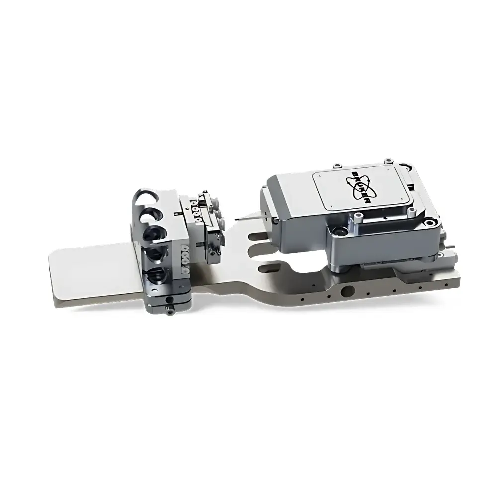
Bruker PI 89 In-Situ SEM Nanoindenter System
| Brand | Bruker |
|---|---|
| Origin | USA |
| Manufacturer Type | Authorized Distributor |
| Origin Category | Imported |
| Model | PI 89 |
| Pricing | Available Upon Request |
Overview
The Bruker PI 89 In-Situ SEM Nanoindenter System is a high-precision, modular nanomechanical testing platform engineered for real-time, quantitative mechanical characterization inside scanning electron microscopes (SEM) and focused ion beam–SEM (FIB/SEM) chambers. Leveraging Bruker’s proprietary capacitive displacement sensing architecture—originally developed by Hysitron—the PI 89 enables synchronized imaging and mechanical testing at sub-10 nm spatial resolution and sub-100 nN force resolution. Unlike conventional ex-situ nanoindentation systems, the PI 89 operates within the vacuum environment of the SEM, permitting direct correlation between microstructural evolution (e.g., dislocation nucleation, crack propagation, phase transformation) and mechanical response under controlled load/displacement conditions. Its design adheres to fundamental principles of contact mechanics (Oliver–Pharr method), dynamic indentation theory, and fracture mechanics, making it suitable for research-grade materials science, thin-film reliability assessment, and advanced semiconductor packaging development.
Key Features
- Multi-range capacitive transducer options: 10 mN, 500 mN, 3.5 N, and 150 µm displacement capacity—enabling seamless transition from nanoscale indentation to microscale compression/tension.
- Performech® II advanced control module with 78 kHz closed-loop feedback bandwidth and 39 kHz data acquisition rate—capable of resolving transient events such as brittle fracture initiation, pop-in phenomena, and cyclic fatigue crack nucleation.
- Patented rotational and tilt sample stages—allowing precise angular repositioning during in-situ FIB milling, secondary electron imaging, and multi-axis mechanical loading without breaking vacuum.
- Modular functional expansion: integrated electrochemical module (ECM), film-to-wire pull-to-push (PTP) conversion stage, direct tensile testing capability, high-temperature stage (up to 800 °C), nanoscratch module, and SPM-compatible XPM (mechanical property mapping) functionality.
- Encoder-based sample stage with 1 nm positional resolution—enabling grain-specific indentation within polycrystalline microstructures and targeted probing of phase boundaries or interfacial regions.
Sample Compatibility & Compliance
The PI 89 accommodates standard SEM stubs (e.g., 12.7 mm, 25 mm diameter) and custom TEM grid-compatible holders. It supports conductive and non-conductive samples—including metallic alloys, ceramics, polymers, thin-film stacks, nanowires, and 2D materials—with optional charge compensation protocols. The system complies with ISO 14577 (metallic materials—instrumented indentation testing), ASTM E2546 (standard guide for instrumented indentation testing), and supports GLP/GMP-aligned audit trails when integrated with Bruker’s NanoTest™ software suite. All firmware and control logic are designed to meet electromagnetic compatibility (EMC) Class B requirements per EN 61326-1 for laboratory environments.
Software & Data Management
Control and analysis are performed via Bruker’s NanoTest™ software, which provides fully scriptable test sequences, real-time force–displacement curve overlay with SEM image synchronization, and automated feature-tracking algorithms for strain-field mapping. Data export conforms to ASTM E1436-compliant ASCII formats and HDF5 binary structures, ensuring interoperability with MATLAB®, Python (via h5py), and commercial finite element postprocessors. The software supports 21 CFR Part 11-compliant electronic signatures, user role-based access control, and full audit trail logging—including operator ID, timestamp, parameter changes, and raw sensor output—for regulated R&D and quality assurance workflows.
Applications
- In-situ deformation studies of grain boundaries and twin boundaries in Ni-based superalloys and Mg alloys.
- Interfacial adhesion quantification in Cu/low-k dielectric stacks for advanced node IC packaging.
- Mechanical stability assessment of ALD-grown oxide layers under thermal cycling (via integrated 800 °C heating stage).
- Fatigue life modeling of MEMS structural films using high-frequency cyclic loading (1–100 Hz) with simultaneous SE/BSE imaging.
- Nanoscale scratch resistance evaluation of protective DLC coatings on biomedical implants.
- Correlative nanomechanics–chemistry: simultaneous ECM + nanoindentation for stress-corrosion cracking investigations in stainless steels.
FAQ
Is the PI 89 compatible with all SEM/FIB-SEM platforms?
Yes—mechanical and electrical integration kits are available for Thermo Fisher Scientific, Zeiss, JEOL, and Hitachi systems; custom interfacing is supported via Bruker’s OEM engineering team.
Can the system perform true uniaxial tensile tests at the nanoscale?
Yes—the dedicated direct-tension module enables displacement-controlled uniaxial loading of freestanding nanowires and micropillars with active load feedback and real-time strain measurement.
What vacuum level is required for stable operation?
The PI 89 operates reliably down to 1 × 10⁻⁴ Pa (10⁻⁶ Torr); no additional vacuum pumping is required beyond standard SEM chamber specifications.
How is calibration traceability maintained?
Force calibration follows NIST-traceable reference standards (SRM 2241, SRM 2242); displacement calibration uses laser interferometry validated against PTB/NPL protocols.
Does the system support third-party automation or API integration?
Yes—RESTful API endpoints and Python SDK are provided for integration into automated materials discovery workflows and digital lab infrastructure (e.g., LabArchives, ELN systems).


