CDE ResMap 168 Automated Four-Point Probe Sheet Resistance & Resistivity Mapping System
| Brand | CDE ResMap |
|---|---|
| Origin | USA |
| Model | ResMap 168 |
| Automation Level | Fully Automated |
| Probe Material | Tungsten Carbide (WC) |
| Probe Lifetime | >500,000 measurements |
| Vertical Resolution for Probe Contact Optimization | 0.01 mm |
| Measurement Range | 1 mΩ/□ to 5 MΩ/□ |
| Standard Reference Wafers Included | NIST-traceable calibration set (6 pieces) |
Overview
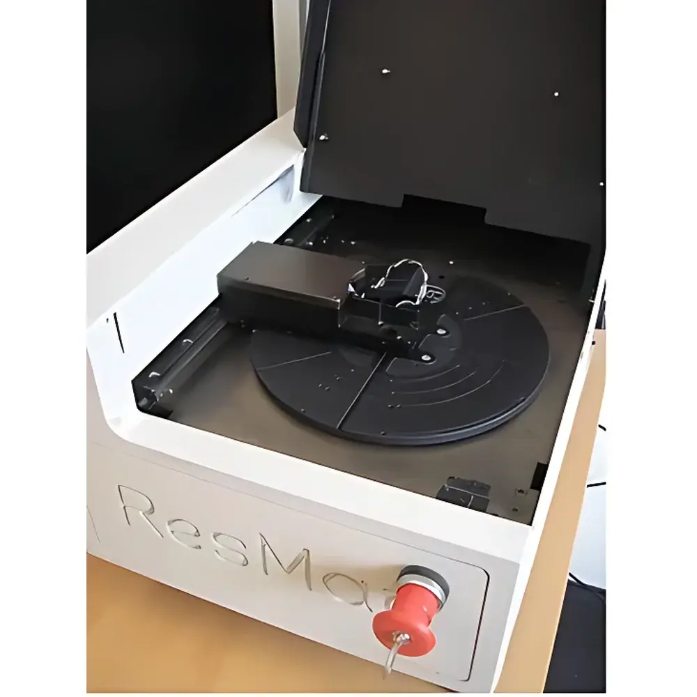
The CDE ResMap 168 is a fully automated, high-precision four-point probe mapping system engineered for quantitative sheet resistance (Rs) and bulk resistivity (ρ) characterization of planar semiconductor and thin-film photovoltaic materials. Operating on the established van der Pauw and linear four-point probe principles—where current is forced through two outer probes and voltage sensed across two inner probes—the ResMap 168 eliminates contact resistance errors and delivers traceable, geometry-independent measurements. Designed specifically for high-throughput production environments in solar cell manufacturing, it integrates motorized X-Y-Z stage control, real-time probe force feedback, and software-driven contact optimization to ensure consistent, non-destructive probing across fragile or heterogeneous surfaces—including amorphous silicon (a-Si), microcrystalline silicon (μc-Si), transparent conductive oxides (TCOs), selective emitters, passivated contacts (e.g., SiOx/a-Si:H stacks), and electroplated copper electrodes. Its architecture conforms to fundamental metrology requirements for process development, inline QC, and yield analysis in ISO 9001- and IEC 61215-compliant PV fabrication lines.
Key Features
- Fully automated wafer handling with integrated conveyor interface—enables unattended batch processing of standard 156 mm × 156 mm to 210 mm × 210 mm wafers or substrates up to 300 mm diameter.
- Patented CDE probe-contact optimization algorithm: dynamically adjusts probe touchdown depth (0.01 mm resolution) based on material hardness, film stack compliance, and ion implantation depth—eliminating manual mechanical recalibration.
- Tungsten carbide (WC) probe array with >500,000 measurement cycle lifetime; wear-compensated tip geometry ensures stable contact area and minimal surface damage on soft films or textured surfaces.
- NIST-traceable calibration suite included (6 certified reference wafers) supporting internal verification, drift monitoring, and audit-ready documentation per ISO/IEC 17025 requirements.
- Real-time thermal drift compensation and auto-zeroing circuitry maintain measurement stability over extended runs (>8 h continuous operation) without recalibration.
- Modular probe head design compatible with optional temperature-controlled chucks (−40 °C to +150 °C) for temperature-dependent resistivity profiling.
Sample Compatibility & Compliance
The ResMap 168 supports rigid and semi-flexible substrates ranging from 0.1 mm to 5 mm thickness, including monocrystalline and multicrystalline silicon wafers, glass-based TCO layers, polymer-supported metal grids, and heterojunction test coupons. It meets ASTM F390-22 (Standard Test Methods for Sheet Resistance of Semiconductor Materials Using Four-Point Probes) and aligns with SEMI PV22-0718 (Test Method for Sheet Resistance Uniformity of Silicon Photovoltaic Wafers). All measurement data logs include full metadata (timestamp, probe force, Z-position, ambient temperature/humidity, operator ID) to satisfy GLP/GMP audit trails and FDA 21 CFR Part 11 electronic record integrity requirements when paired with validated CDE DataVault software.
Software & Data Management
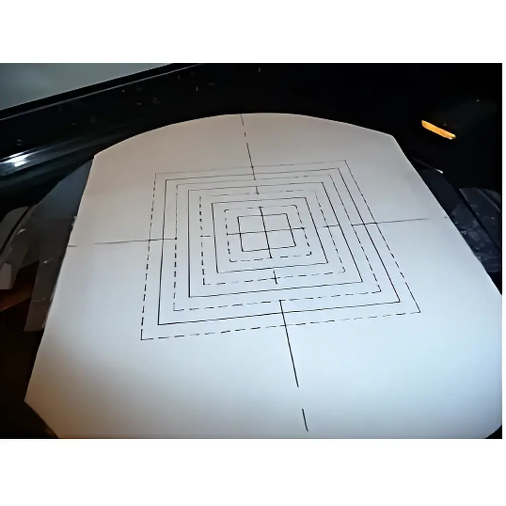
Controlled via CDE MapView™ v5.3, the system provides intuitive GUI navigation, customizable measurement grid definitions (linear, spiral, concentric, or user-defined ROI), and real-time color-coded Rs mapping with statistical overlay (mean, std dev, min/max, uniformity %). Raw data exports to CSV, XML, and HDF5 formats; integrated Python API enables direct integration into factory MES systems (e.g., Siemens Opcenter, Rockwell FactoryTalk). Audit logs record all parameter changes, calibration events, and user actions with digital signature support. Optional CDE DataVault module adds role-based access control, encrypted storage, and automated report generation compliant with ISO 13485 and IATF 16949 documentation standards.
Applications
- Process validation of phosphorus/boron diffusion profiles in selective emitter structures.
- Uniformity assessment of ALD-grown Al2O3 passivation layers prior to firing.
- Quantitative evaluation of plating uniformity and line resistance in Cu-electroplated front-side metallization.
- Characterization of tandem cell interconnect layers (e.g., ITO/ZnO bilayers) for series resistance minimization.
- R&D screening of novel transparent electrodes (Ag nanowires, graphene hybrids, conductive polymers) under controlled environmental conditions.
- Root-cause analysis of edge losses and hotspot formation correlated with localized Rs anomalies.
FAQ
Does the ResMap 168 support measurement of ultra-thin films (<10 nm)?
Yes—when combined with optional low-current sourcing (10 nA–100 µA range) and shielded cabling, it achieves reliable Rs quantification down to ~0.5 nm effective thickness for highly doped films, subject to substrate conductivity constraints.
Can it measure curved or textured surfaces, such as black silicon?
The adaptive Z-control algorithm and spring-loaded probe suspension enable stable contact on surfaces with RMS roughness up to 5 µm; optional tactile sensor feedback further enhances repeatability on pyramid-textured mc-Si.
Is remote diagnostics and firmware update capability available?
Yes—via secure TLS-encrypted Ethernet connection; CDE RemoteAssist allows authorized service engineers to perform health checks, log analysis, and version-controlled updates without onsite intervention.
How is probe-to-probe alignment verified and maintained?
A built-in optical alignment station with 5 µm resolution CCD imaging and motorized stage positioning enables daily verification; alignment certificates are generated and stored with each calibration event.
What regulatory documentation is supplied with shipment?
Each unit ships with Declaration of Conformity (CE/UKCA), NIST-traceable calibration certificate, ISO 17025 scope statement from CDE’s accredited lab, and full technical file per EU MDR Annex II requirements.


