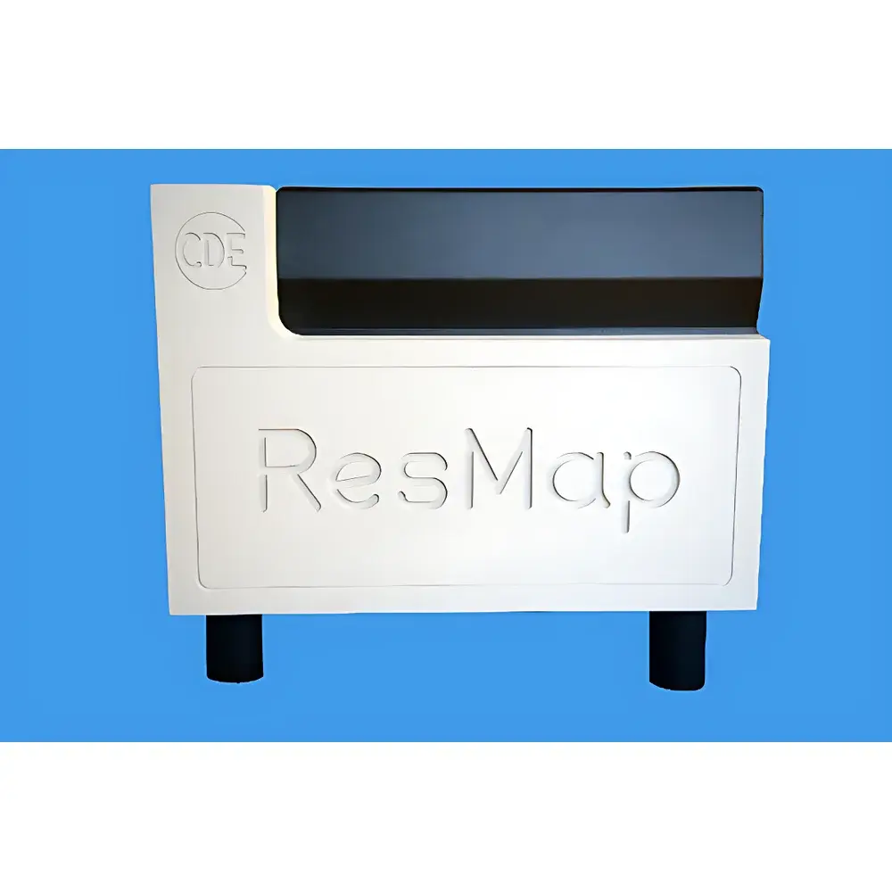
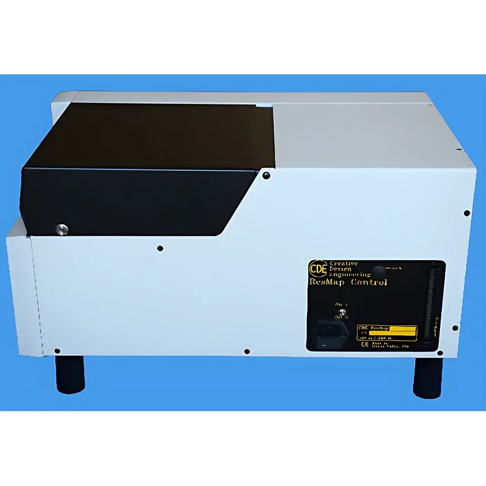
CDE ResMap 273 Four-Point Probe Sheet Resistance & Resistivity Mapping System
| Brand | CDE ResMap |
|---|---|
| Origin | USA |
| Model | ResMap 273 |
| Automation Level | Fully Automatic |
| Price | USD $68,000 |
| Probe Material | Tungsten Carbide (WC) |
| Probe Lifetime | >500,000 touchdowns |
| Standard Calibration Wafers Included | NIST-traceable set of 6 wafers |
| Measurement Range | 1 mΩ/□ to 5 MΩ/□ |
| Vertical Resolution for Probe Landing Control | 0.01 mm (software-adjustable) |
Overview
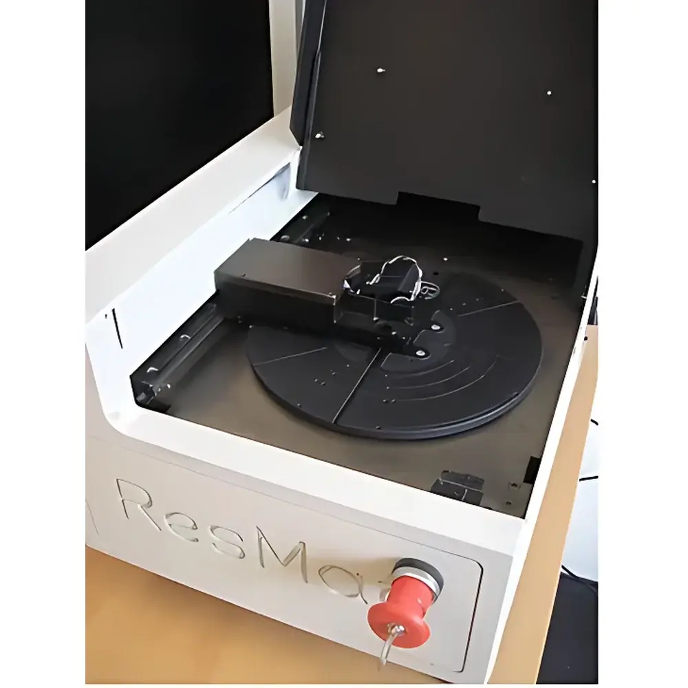
The CDE ResMap 273 is a fully automated, desktop-grade four-point probe resistivity and sheet resistance mapping system engineered specifically for semiconductor process development, photovoltaic R&D, and thin-film metrology. Based on the proven architecture of the ResMap 178 platform, the ResMap 273 extends measurement capability to substrates up to 210 mm in diameter—addressing evolving industry requirements for larger-area solar wafers while maintaining sub-millimeter spatial resolution and high reproducibility. Its compact footprint (designed for benchtop integration in cleanroom or lab environments), rugged mechanical construction, and thermally stable probe head ensure long-term measurement integrity under routine production or research conditions. The instrument operates on the fundamental principle of the four-point collinear probe method, eliminating contact resistance and lead resistance contributions through separate current injection and voltage sensing paths—a technique standardized in ASTM F84–22 and widely adopted for quantitative characterization of doped silicon, amorphous/microcrystalline silicon, transparent conductive oxides (TCOs), metal electrodes, and passivation layers.
Key Features
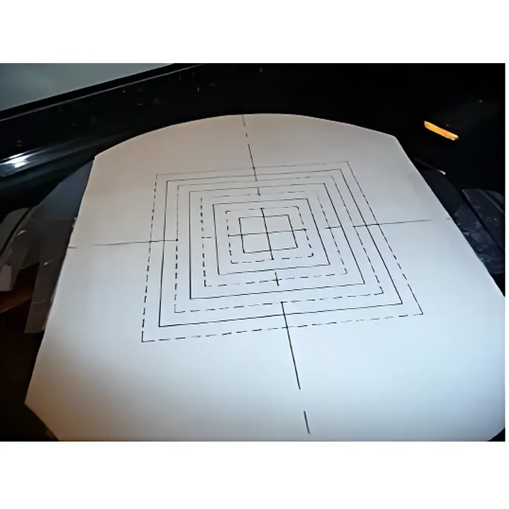
- Fully automated XY stage with programmable scan patterns (grid, radial, edge-to-edge), supporting wafer sizes from 30 mm to 210 mm
- Patented CDE software-controlled probe landing optimization: real-time adjustment of touchdown force and vertical position with 0.01 mm resolution—no manual hardware recalibration required across material types (e.g., soft polymer films, hard ion-implanted Si, or low-k dielectrics)
- Tungsten carbide (WC) probe tips with >500,000 touchdown durability, minimizing maintenance intervals and drift-induced measurement uncertainty
- NIST-traceable calibration suite included (6 certified reference wafers), enabling immediate traceability per ISO/IEC 17025 requirements
- Integrated environmental monitoring: temperature and humidity sensors log ambient conditions alongside each measurement for post-acquisition correction and audit trail compliance
- Compliant with SEMI E10 and E142 standards for equipment qualification and data integrity in semiconductor manufacturing environments
Sample Compatibility & Compliance
The ResMap 273 accommodates flat, rigid substrates including single-crystal silicon, glass, quartz, sapphire, and ceramic carriers. It supports both bare wafers and patterned samples with surface topography variations ≤ ±5 µm over 1 mm². Critical applications include sheet resistance profiling of selective emitters, passivated emitter rear cells (PERC), tunnel oxide passivated contacts (TOPCon), and electroplated copper interconnects. All measurements adhere to ASTM F84–22 (Standard Test Method for Measuring Resistivity of Silicon Wafers Using the Four-Point Probe Technique) and are compatible with GLP/GMP documentation workflows. Instrument firmware includes audit trail functionality compliant with FDA 21 CFR Part 11 for electronic records and signatures, supporting regulated environments in PV cell fabrication and advanced packaging R&D.
Software & Data Management
ResMapControl™ v5.2 software provides intuitive workflow management—from recipe setup and real-time map visualization to statistical process control (SPC) charting and export to CSV, HDF5, or SEMI GEM-compliant SECS/GEM protocols. Each measurement session automatically generates a timestamped metadata file containing probe parameters, environmental logs, calibration status, and operator ID. Data encryption at rest and role-based user access control (admin/operator/viewer) ensure alignment with ISO 27001 information security frameworks. Raw sheet resistance maps can be exported for further analysis in MATLAB, Python (NumPy/SciPy), or JMP; batch processing scripts support automated uniformity reporting (e.g., 3σ, max-min, center-to-edge delta) per wafer lot.
Applications
- Quantitative sheet resistance mapping of phosphorus/boron-diffused emitters and back-surface fields in crystalline silicon solar cells
- Uniformity assessment of ALD-sputtered ITO, AZO, and FTO layers on glass or flexible substrates
- Process validation of laser doping, inkjet-printed electrodes, and electrochemical metallization steps
- Correlation studies between sheet resistance gradients and minority carrier lifetime (via μ-PCD or PL imaging)
- Qualification of surface passivation quality on SiNx:H or Al₂O₃-coated wafers using low-current, high-impedance probing modes
- Research into novel 2D materials (e.g., graphene, MoS₂) where contact resistance minimization is critical for accurate carrier concentration estimation
FAQ
Does the ResMap 273 require physical recalibration when switching between different substrate materials?
No—its patented software-driven probe landing optimization adjusts touchdown parameters dynamically based on material hardness and surface morphology, eliminating manual recalibration.
Is the system compatible with non-standard wafer shapes or irregular substrates?
It supports only flat, circular or square rigid substrates within the defined size range (30–210 mm); non-planar or flexible roll-to-roll samples require custom fixturing not supplied standard.
How is measurement traceability maintained over time?
Each system ships with six NIST-traceable calibration wafers; periodic verification against these references—logged with timestamps and operator IDs—fulfills ISO/IEC 17025 internal audit requirements.
Can raw voltage/current data be accessed for custom algorithm development?
Yes—full digitized analog front-end outputs (Vsense, Idrive) are available via API interface for advanced modeling or machine learning integration.
What level of training and technical support is provided with purchase?
CDE offers onsite installation, two-day operator certification, and annual remote calibration verification services; extended warranty and SLA-backed response times are available under service contracts.


