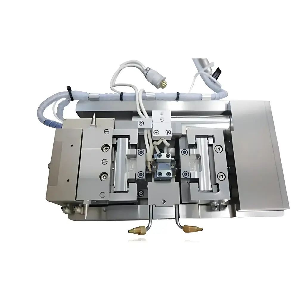
Deben MICROTEST In-Situ Dynamic Tensile Testing Stage for SEM
| Key | Origin: USA |
|---|---|
| Manufacturer | Deben Ltd. |
| Distributor | Optosky Co., Ltd. |
| Type | Imported |
| Model | MICROTEST |
| Load Capacity Options | 200 N, 300 N, 2000 N, 5000 N |
| Strain Rate Range | 5 µm/min – 6 mm/min |
| Force Sensor Resolution | Down to 2 N |
| Bending Configurations | Horizontal 3-point & 4-point |
| EBSD-Compatible Versions | MICROTEST2000ES/EW, MICROTEST5000S/W |
| Thermal Options | RT, Heated (EH2000/H5000), Water-Cooled (MICROTEST2000W/5000W) |
| Software | Real-time stress–strain plotting with threshold-triggered acquisition and synchronized image–data capture |
Overview
The Deben MICROTEST In-Situ Dynamic Tensile Testing Stage is a precision-engineered mechanical testing platform designed exclusively for integration within scanning electron microscope (SEM) chambers. It enables real-time, high-resolution observation of microstructural evolution—such as dislocation activity, crack nucleation and propagation, grain rotation, phase transformation, and interfacial decohesion—during controlled uniaxial tensile, compressive, or bending deformation. Operating on the principle of direct-load application via piezoelectric or motor-driven actuation coupled with calibrated load cell feedback, the MICROTEST system maintains sub-micron displacement resolution and high force reproducibility under vacuum-compatible conditions (typically ≤10⁻⁴ mbar). Its modular architecture supports both room-temperature and thermally regulated experiments—including EBSD-compatible configurations—making it a foundational tool for quantitative in-situ micromechanics in materials science laboratories adhering to ASTM E8/E9, ISO 6892-1, and USP mechanical testing guidelines.
Key Features
- Four scalable load capacity variants: MICROTEST200 (200 N), MICROTEST300 (300 N), MICROTEST2000 (2000 N), and MICROTEST5000 (5000 N), each validated for operation inside and outside the SEM chamber.
- Interchangeable load cells with selectable ranges down to 2 N, enabling high-sensitivity measurement for low-force regimes (e.g., thin films, nanowires, biological scaffolds).
- Precisely programmable strain rates from 5 µm/min to 6 mm/min, supporting quasi-static to moderate-rate deformation protocols.
- Dual-axis bending capability: horizontal 3-point and 4-point fixtures; vertical 3-point bending (MICROTEST200B and MICROTEST2000B models) for constrained geometry studies.
- EBSD-optimized versions (MICROTEST2000ES/EW, MICROTEST5000S/W) feature low-outgassing materials, minimized electromagnetic interference, and precise sample tilt compatibility (±10°) for crystallographic mapping during deformation.
- Thermal modules include resistive heating (EH2000/H5000 upgrades), water-cooled stages (MICROTEST2000W/5000W), and dual-mode heating/cooling configurations for thermo-mechanical coupling studies.
- Integrated digital control interface with real-time stress–strain curve rendering, user-defined trigger thresholds (e.g., load drop, displacement step), and automated event-based image capture synchronization.
Sample Compatibility & Compliance
The MICROTEST stage accommodates standard SEM stubs (e.g., 12.7 mm pin-mount, 25 mm flat-mount) and accepts custom sample geometries up to 15 mm in gauge length. It is routinely deployed for metals (Al, Ti, Ni alloys), ceramics (Al₂O₃, SiC), polymers (PEEK, PET), composites (CFRP, MMCs), geological specimens (basalt, ice cores), and coated systems (PVD/CVD thin films on metallic substrates). All variants comply with SEM vacuum requirements (UHV-compatible seals, low-vapor-pressure lubricants) and meet CE safety directives. Force calibration traceability follows ISO/IEC 17025-accredited procedures, and data audit trails satisfy GLP/GMP documentation standards per FDA 21 CFR Part 11 when used with validated software configurations.
Software & Data Management
The MICROTEST Control Suite provides deterministic real-time acquisition of load, displacement, and environmental parameters (temperature, vacuum level) at up to 1 kHz sampling rate. Stress–strain curves are plotted live with automatic yield point detection, modulus calculation (tangent/secant), and hysteresis loop analysis for cyclic loading. Synchronized image acquisition integrates natively with common SEM imaging platforms (e.g., Zeiss SmartSEM, Thermo Fisher Avizo, JEOL JSM-IT series) via TTL or Ethernet triggers. Export formats include CSV, HDF5, and XML for post-processing in MATLAB, Python (NumPy/Pandas), or commercial finite element pre-processors. Audit logs record operator ID, timestamp, parameter set, and hardware configuration—essential for regulatory submissions and inter-laboratory method transfer.
Applications
- Metallic systems: In-situ tracking of slip band formation, twin boundary migration, stress-induced martensitic transformation, and coating delamination kinetics under thermal–mechanical cycling.
- Composites & fibers: Quantification of fiber–matrix load transfer efficiency, interfacial debonding onset, and progressive damage accumulation in CFRP laminates.
- Polymers & biomaterials: Observation of crazing, shear yielding, and void coalescence mechanisms during tensile straining; viscoelastic recovery assessment via hold-relax protocols.
- Ceramics & brittle solids: Direct imaging of microcrack initiation sites, bridging ligament fracture, and R-curve behavior under controlled crack extension.
- Geological & cryogenic samples: Compression of ice cores and rock analogs at sub-zero temperatures to simulate glacial deformation or crustal stress relaxation.
- Thin films & nanostructures: Mechanical characterization of freestanding nanomembranes and MEMS-relevant structures using specialized micro-grippers and alignment fixtures.
FAQ
Is the MICROTEST stage compatible with field-emission SEMs (FE-SEM)?
Yes—its compact footprint, low magnetic signature, and vacuum-compatible construction ensure stable operation in high-resolution FE-SEM environments without signal interference or chamber contamination.
Can I perform simultaneous EBSD and mechanical testing?
Yes—MICROTEST2000ES/EW and MICROTEST5000S/W models are specifically engineered for EBSD integration, featuring optimized sample tilt geometry, minimal shadowing, and synchronized pattern acquisition triggers.
What is the maximum operating temperature for heated configurations?
Standard EH2000 and H5000 upgrades support up to 800 °C; custom high-temperature variants (up to 1200 °C) are available upon request with tungsten-based heating elements and ceramic insulation.
Does the system support closed-loop displacement or load control?
All MICROTEST models operate in closed-loop mode using PID-regulated actuation, with user-selectable control variable (load, displacement, or strain) and real-time feedback from integrated sensors.
How is data synchronization between SEM images and mechanical signals achieved?
Via hardware-level TTL pulse triggering or software-based time-stamped metadata embedding, ensuring sub-millisecond alignment accuracy across modalities for quantitative structure–property correlation.


