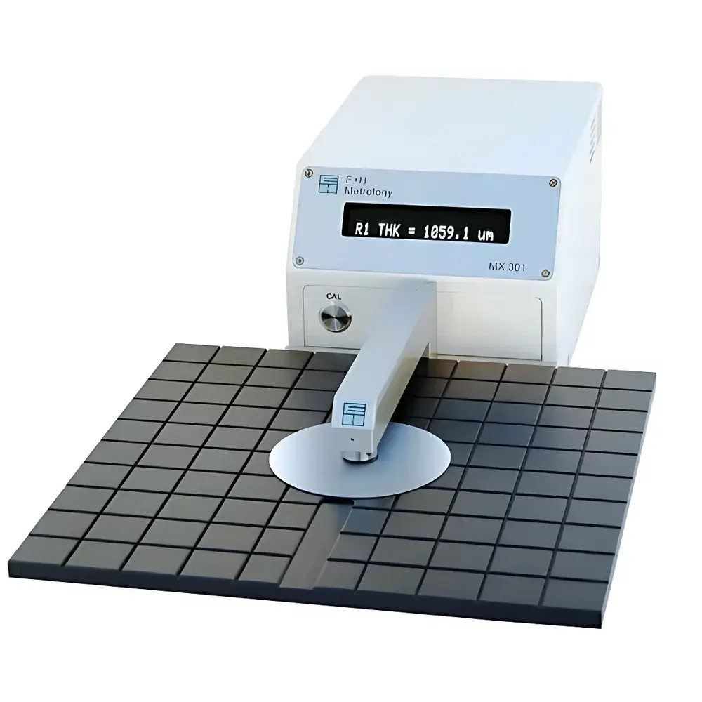
E+H Metrology MX 301 Non-Contact Single-Point Wafer Thickness Gauge
| Brand | E+H Metrology |
|---|---|
| Origin | Germany |
| Model | MX 301 |
| Wafer Diameters Supported | 50 mm, 75 mm, 100 mm, 150 mm, 200 mm, 300 mm |
| Thickness Accuracy | ±0.5 µm |
| Resolution | 10 nm |
| Dynamic Range | 800 µm |
| Standard Thickness Range | 0–1600 µm |
| Measurement Principle | Dual-Sided Capacitive Distance Sensing |
| Calibration Method | Certified Gauge Blocks |
| Output Interface | RS-232 Serial Interface |
| Display | 5-Digit LED |
Overview
The E+H Metrology MX 301 is a high-precision, non-contact single-point wafer thickness gauge engineered for semiconductor process control and quality assurance laboratories. It implements a dual-capacitive sensing architecture—where two calibrated capacitive displacement sensors are rigidly mounted in opposing positions above and below the wafer—to determine thickness as the sum of two independent, sub-micron distance measurements. This principle eliminates mechanical contact, thermal loading, or surface deformation risks inherent in stylus-based or optical interferometric systems. The MX 301 is optimized for routine thickness verification of bare and processed wafers—including Si, SiC, GaN, GaAs, and InP substrates—across standard diameters from 50 mm to 300 mm. Its design adheres to metrological traceability requirements defined in ISO/IEC 17025 and supports integration into GLP- and GMP-compliant environments where documented measurement uncertainty and calibration history are mandatory.
Key Features
- Dual-sensor capacitive measurement system providing intrinsic immunity to wafer surface reflectivity, roughness, or coating interference
- Stable mechanical frame with thermally compensated sensor mounts ensuring long-term repeatability (≤0.1 µm 24-hour drift under controlled lab conditions)
- 10 nm resolution and ±0.5 µm total system accuracy (including environmental and calibration uncertainty contributions), validated per ISO 10360-2
- Adjustable sensor spacing accommodates wafers up to 1600 µm nominal thickness; dynamic range of 800 µm per sensor enables robust operation across thin-film and bulk substrate geometries
- Integrated 5-digit LED display with real-time thickness readout and status indicators for sensor alignment, signal stability, and out-of-range conditions
- RS-232 serial interface compliant with EIA/TIA-232-E standards for direct connection to SPC software, MES platforms, or custom LabVIEW-based data acquisition systems
- Factory-calibrated using NIST-traceable gauge blocks; user-performed verification and adjustment supported via standardized calibration procedure documented in the instrument’s technical manual
Sample Compatibility & Compliance
The MX 301 is compatible with flat, rigid semiconductor wafers meeting SEMI MW108 and SEMI MF1530 specifications for warpage and total thickness variation (TTV). It supports unpatterned and patterned wafers with front-side films ≤5 µm thick (e.g., SiO₂, SiNₓ, photoresist) without requiring software compensation. Backside roughness (Ra) up to 0.8 µm does not degrade measurement fidelity. The instrument complies with CE marking requirements (2014/30/EU EMC Directive and 2014/35/EU Low Voltage Directive), and its electrical safety design conforms to IEC 61010-1:2010. For regulated manufacturing environments, audit-ready calibration records, firmware version logs, and operator access controls can be maintained externally via host-system integration—supporting alignment with FDA 21 CFR Part 11 electronic record requirements when paired with validated software infrastructure.
Software & Data Management
While the MX 301 operates autonomously via its front-panel interface, it delivers ASCII-formatted measurement data (e.g., “THK=1234.56µmrn”) over RS-232 at configurable baud rates (9600–115200). No proprietary driver is required; standard terminal emulators or Python/Node.js serial libraries enable immediate integration. Optional E+H Metrology DataLink utility (v3.2+) provides timestamped CSV export, statistical process monitoring (X̄ & R charts), and automated pass/fail flagging against user-defined upper/lower specification limits. All exported datasets include embedded metadata: instrument ID, firmware revision, calibration date, ambient temperature (measured via onboard sensor), and operator ID (if entered manually). Raw data files comply with ASTM E2795-21 guidelines for metrological data archiving.
Applications
- Post-lapping and post-polishing thickness validation in wafer fabrication fabs
- Lot acceptance testing for epitaxial layer growth uniformity on compound semiconductor substrates
- In-process monitoring during chemical mechanical planarization (CMP) development trials
- Reference thickness measurement for calibrating inline optical metrology tools (e.g., spectroscopic reflectometers)
- Research-grade thickness profiling of ultra-thin (<50 µm) SiC and GaN handle wafers used in power device manufacturing
- Quality gate verification prior to wafer bonding or heteroepitaxial transfer processes
FAQ
Does the MX 301 require periodic recalibration by an accredited lab?
Yes—E+H Metrology recommends annual recalibration by an ISO/IEC 17025-accredited laboratory using certified gauge blocks traceable to national metrology institutes. Internal verification with customer-owned standards should be performed before each shift.
Can the MX 301 measure warped or bowed wafers?
It measures local thickness at the single point aligned between the two sensors. For wafers exceeding ±25 µm bow (per SEMI MF1530), positional repeatability may degrade; use only on wafers within specified TTV limits.
Is vacuum or nitrogen purging supported for inert-atmosphere measurements?
No—the MX 301 is designed for ambient air operation. Capacitive sensing is unaffected by atmospheric composition, but relative humidity >80% RH may require extended stabilization time.
What is the warm-up time required for specified accuracy?
Minimum 30 minutes after power-on at stable lab temperature (20–24 °C); full thermal equilibrium achieved after 60 minutes.
How is sensor alignment verified?
Via built-in self-test mode that reports differential zero-offset drift between upper and lower sensors; alignment tolerance is ±2 µm lateral misalignment and <0.1° angular deviation.


