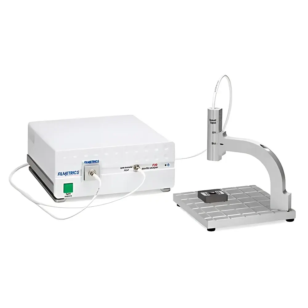
Filmetrics F20 Single-Point Thin-Film Thickness Measurement System
| Brand | Filmetrics |
|---|---|
| Model | F20 |
| Measurement Principle | Spectroscopic Reflectometry |
| Thickness Range | 1 nm – 10 mm (material-dependent) |
| Wavelength Range | Configurable from 190–1700 nm (model-specific) |
| Interface | USB 2.0 |
| Sample Stage | Manual XYZ-adjustable |
| Software | Filmetrics F20 Control & Analysis Suite v5.x |
| Compliance | Compatible with ASTM E1938, ISO 9276-2, and GLP/GMP data integrity workflows (audit trail, user access control, electronic signatures per FDA 21 CFR Part 11) |
| Power | 100–240 VAC, 50/60 Hz |
| Dimensions | 24 × 18 × 12 cm (L×W×H) |
| Weight | 3.2 kg |
Overview
The Filmetrics F20 is a benchtop spectroscopic reflectometer engineered for rapid, non-contact, single-point thickness and optical constant characterization of transparent and semi-transparent thin films. It operates on the principle of broadband spectral reflectance analysis: a collimated white light beam (UV-VIS-NIR, depending on configuration) is directed onto the sample surface at near-normal incidence; the reflected spectrum is captured by a high-resolution spectrometer and compared against theoretical Fresnel-based models via real-time least-squares fitting. This physics-based inversion enables simultaneous determination of film thickness, refractive index (n), extinction coefficient (k), reflectance (R), transmittance (T), and uniformity—without requiring prior knowledge of substrate or film dispersion. Designed for integration into R&D labs, QC environments, and pilot-line process monitoring, the F20 delivers sub-nanometer thickness resolution on smooth, low-absorption dielectrics and semiconductors, with measurement times under 2 seconds per point after calibration.
Key Features
- Modular optical head architecture supporting six wavelength-configured variants (F20, F20-EXR, F20-NIR, F20-UV, F20-UVX, F20-XT) to match material absorption edges and thickness regimes
- High-fidelity spectral acquisition (0.2–1.5 nm optical resolution, 1024-pixel CCD or InGaAs array) enabling robust modeling of interference fringes across 1 nm–10 mm thickness range
- Integrated motorized XYZ stage (optional) for automated mapping of thickness uniformity across wafers or substrates up to 200 mm diameter
- Filmetrics F20 Software v5.x with intuitive workflow-driven interface: auto-alignment guidance, multi-layer stack modeling (up to 10 layers), dispersion fitting (Cauchy, Sellmeier, Tauc-Lorentz), and batch report generation in PDF/CSV/XLSX
- FDA 21 CFR Part 11-compliant software mode featuring electronic signatures, role-based user permissions, immutable audit trails, and secure data export for regulated environments (ISO 13485, ICH Q5, USP )
- Compact footprint (24 × 18 × 12 cm), USB 2.0 plug-and-play connectivity, and minimal warm-up time (<60 s)
Sample Compatibility & Compliance
The F20 accommodates rigid and flexible substrates—including silicon wafers, fused silica, BK7 glass, PET, PI, and quartz—with surface roughness <5 nm RMS. It measures single-layer and multilayer stacks (e.g., SiO₂/TiO₂ anti-reflection coatings, ITO/polymer OLED electrodes, DLC hard coatings, SU-8 photoresist, amorphous silicon PV layers, CIGS absorbers). Films must exhibit sufficient optical contrast and minimal scattering; typical measurable materials include oxides (SiO₂, Al₂O₃, Ta₂O₅), nitrides (Si₃N₄, TiN), polymers (PMMA, PDMS, parylene-C), chalcogenides (GeSbTe), and transparent conductive oxides (ITO, AZO, FTO). The system complies with ASTM E1938 (Standard Practice for Measuring Thickness of Transparent Films Using Spectroscopic Reflectometry) and supports traceable calibration using NIST-traceable reference standards. All measurement data adhere to GLP and GMP documentation requirements when configured in compliance mode.
Software & Data Management
Filmetrics F20 Control & Analysis Suite provides full metrology lifecycle management: instrument initialization, optical alignment validation, model definition (layer sequence, material libraries, dispersion models), measurement execution, real-time curve fitting, uncertainty estimation, and statistical reporting. Raw spectra and fitted parameters are stored in a structured SQLite database with timestamping, operator ID, and environmental metadata (ambient temperature/humidity if logged externally). Export options include ASCII, CSV, Excel, and PDF reports compliant with ISO/IEC 17025 clause 7.8. Audit logs record every user action—including parameter edits, model changes, and report exports—with cryptographic hashing to prevent tampering. Optional API (DLL/.NET) enables integration into MES, LIMS, or custom automation frameworks.
Applications
The F20 serves critical roles across semiconductor fabrication (gate oxide, ARC, and passivation layer QC), flat-panel display manufacturing (ITO thickness uniformity on TFT arrays), photovoltaics (anti-reflective coating optimization on c-Si and perovskite cells), biomedical device development (hydrogel thickness on biosensor surfaces), optical coating R&D (multilayer filter design verification), and MEMS packaging (capping layer integrity assessment). It is routinely deployed for process development feedback (e.g., PECVD, sputtering, spin-coating), incoming material inspection, and failure analysis (delamination, etch depth quantification, post-annealing densification).
FAQ
What film thickness ranges does the F20 support?
Thickness measurement capability spans 1 nm to 10 mm, depending on film material, optical constants, and selected wavelength configuration (e.g., F20-UV achieves 1 nm resolution on SiO₂; F20-XT resolves >100 µm polymer films on IR-transparent substrates).
Can the F20 measure rough or patterned surfaces?
It requires optically smooth surfaces (Ra < 5 nm); highly textured, porous, or nanostructured films introduce scattering that degrades spectral fidelity and model convergence.
Is vacuum or inert atmosphere operation supported?
The standard F20 is designed for ambient air operation; optional environmental chambers (temperature-controlled or nitrogen-purged) can be integrated for moisture-sensitive or thermally unstable films.
How is calibration performed?
Factory calibration uses NIST-traceable Si/SiO₂ reference wafers; end-users perform daily verification with certified thickness standards; no consumables or recalibration services are required within the 2-year warranty period.
Does the system support automated wafer mapping?
Yes—when equipped with the optional motorized XY stage and F20 Mapping Module, it performs full-wafer thickness uniformity scans with sub-10 µm positional repeatability and automated report generation per SEMI MF1530.