Filmetrics F50 Thin-Film Thickness Measurement System
| Brand | KLA |
|---|---|
| Origin | USA |
| Model | Filmetrics F50 |
| Measurement Principle | Broadband Spectral Reflectometry |
| Maximum Sample Diameter | 450 mm |
| Stage Type | Motorized R-Theta Platform |
| Scan Patterns | Polar, Rectangular, Linear, and User-Defined |
| Wavelength Options | UV–NIR (model-dependent, e.g., F50-UV: 190–1100 nm |
| F50-NIR | 900–1700 nm) |
| Measurement Speed | Up to 2 points per second |
| Predefined Scan Templates | >30 built-in |
| Compliance | Designed for ISO/IEC 17025-aligned lab environments, supports audit-ready data logging per FDA 21 CFR Part 11 requirements when integrated with validated software configuration |
Overview
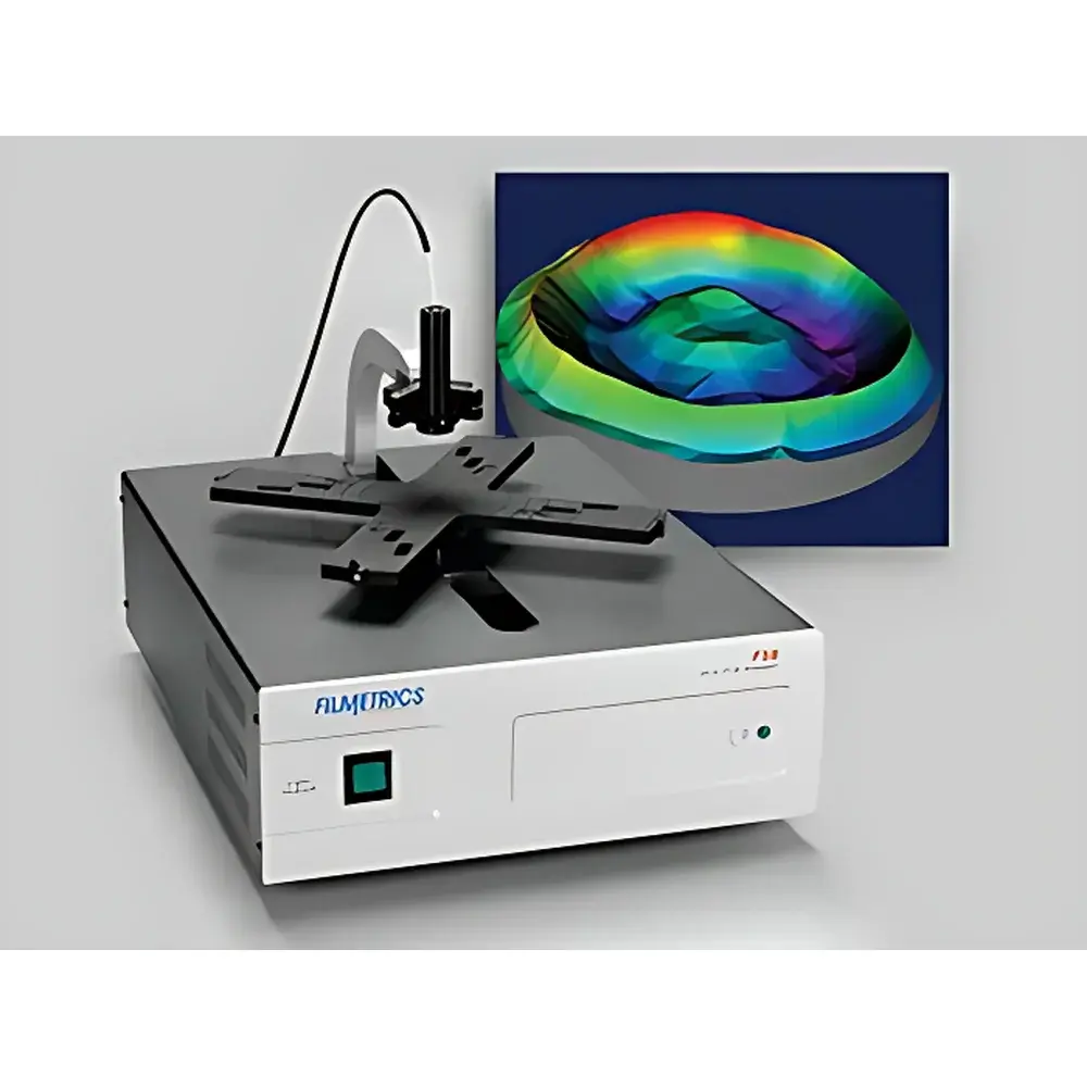
The Filmetrics F50 Thin-Film Thickness Measurement System is a benchtop spectral reflectometry instrument engineered for non-contact, high-reproducibility thickness characterization of single- and multi-layer thin films. Developed by KLA—a global leader in process control and yield management for semiconductor and advanced materials manufacturing—the F50 operates on the physical principle of broadband optical interference analysis. By directing collimated white light onto the sample surface and analyzing the wavelength-dependent intensity distribution of the reflected spectrum, the system solves the film thickness and optical constants (n, k) via rigorous least-squares fitting against Fresnel-based optical models. This method enables sub-nanometer resolution for transparent or semi-transparent dielectrics (e.g., SiO₂, Si₃N₄, photoresists), and robust performance on opaque, rough, or multilayer stacks—including metal/dielectric combinations—when configured with appropriate wavelength modules. The system is optimized for R&D labs, process development centers, and quality control environments where traceable, operator-independent metrology is required without vacuum or destructive sampling.
Key Features
- Motorized R-Theta stage with ±0.001° angular resolution and 450 mm maximum wafer/film substrate compatibility—designed for long-term stability and >1 million repeatable measurement cycles.
- Modular optical head architecture supporting interchangeable wavelength ranges: F50-UV (190–1100 nm) for ultra-thin films (<5 nm), F50-VIS (400–1000 nm) for standard semiconductor and optical coatings, and F50-NIR (900–1700 nm) for thick, absorbing, or scattering layers (e.g., poly-Si, ITO, organic photovoltaics).
- Real-time spectral acquisition at up to 2 measurement points per second, enabling rapid mapping without compromising spectral fidelity or signal-to-noise ratio.
- Flexible scan definition: Polar (radial + angular), Cartesian grid, linear line scans, or fully customizable user-defined coordinate sequences—no hard limit on number of measurement points per map.
- Onboard library of >30 preconfigured measurement templates aligned with common industry workflows (e.g., edge exclusion, center-to-edge profiling, quadrant averaging) and ASTM E2581-compliant reporting structures.
Sample Compatibility & Compliance
The F50 accommodates rigid and semi-rigid substrates including silicon wafers (up to 450 mm), glass slides, quartz plates, sapphire, polymer films (PET, PI), and metal foils. It measures films ranging from 50 µm (e.g., thick polymer encapsulants), provided sufficient optical contrast exists between layers. Surface roughness tolerance extends to Ra ≤ 100 nm for reliable modeling convergence. The system complies with ISO/IEC 17025 documentation practices for calibration traceability and supports GLP/GMP-aligned operation when paired with validated software configurations. Instrument firmware and data handling protocols are architected to meet foundational requirements of FDA 21 CFR Part 11 for electronic records and signatures—enabling secure user authentication, audit trails, and immutable result archiving when deployed in regulated environments.
Software & Data Management
Filmetrics’ proprietary F50 Control Software provides full instrument orchestration, real-time spectral visualization, layer stack modeling, and automated report generation. It includes an embedded optical constant database (refractive index n and extinction coefficient k) for >150 materials across UV–NIR, with support for custom material definitions and dispersion modeling (Cauchy, Sellmeier, Tauc-Lorentz). Data export conforms to ASTM E2581 Annex A1 standards, delivering CSV, XML, and PDF reports with metadata (timestamp, operator ID, calibration status, model parameters, confidence metrics). Raw spectra and fitted residuals are retained with full versioning. Integration with LIMS and MES platforms is supported via OPC UA and RESTful API interfaces, enabling seamless data flow into enterprise quality systems.
Applications
- Semiconductor front-end process control: gate oxide, high-k dielectrics, ALD/CVD film uniformity mapping.
- Display manufacturing: ITO, MoO₃, and metal oxide TFT layer thickness and stoichiometry verification.
- Optical coating QA: anti-reflective, beam-splitter, and filter stack composition and thickness uniformity.
- Photovoltaics: CIGS, perovskite, and SiNx passivation layer metrology during R2R or batch processing.
- MEMS and packaging: polymer underfill, BCB, and PI thickness validation prior to dicing or bonding.
- Academic research: in-situ and ex-situ growth monitoring, interfacial reaction kinetics, and degradation studies.
FAQ
What optical models does the F50 use for thickness calculation?
The system employs rigorously validated transfer-matrix formalism based on Fresnel equations, incorporating substrate effects, surface roughness convolution, and wavelength-dependent dispersion models.
Can the F50 measure films on opaque or highly scattering substrates?
Yes—when equipped with NIR optics (F50-NIR), it characterizes films on metals, ceramics, and textured surfaces by leveraging longer wavelengths that penetrate deeper into scattering media.
Is calibration required before each measurement session?
No routine recalibration is needed; the system uses factory-characterized reference standards and drift-compensated spectral referencing. Annual NIST-traceable verification is recommended per ISO/IEC 17025.
Does the software support multi-layer stack analysis?
Yes—it solves for thickness and optical constants of up to 10 sequential layers simultaneously, with constraints for fixed n/k or thickness ratios.
How is measurement uncertainty quantified?
Each result includes a statistical confidence interval derived from spectral residual analysis, parameter sensitivity matrices, and Monte Carlo propagation of noise and calibration uncertainties.
Related Products


