Gatan MICROTEST 2000E In-Situ Dynamic Tensile Testing Stage
| Origin | USA |
|---|---|
| Manufacturer Type | Authorized Distributor |
| Origin Category | Imported |
| Model | MICROTEST 2000E |
| Price Range | USD 135,000 – 205,000 |
Overview
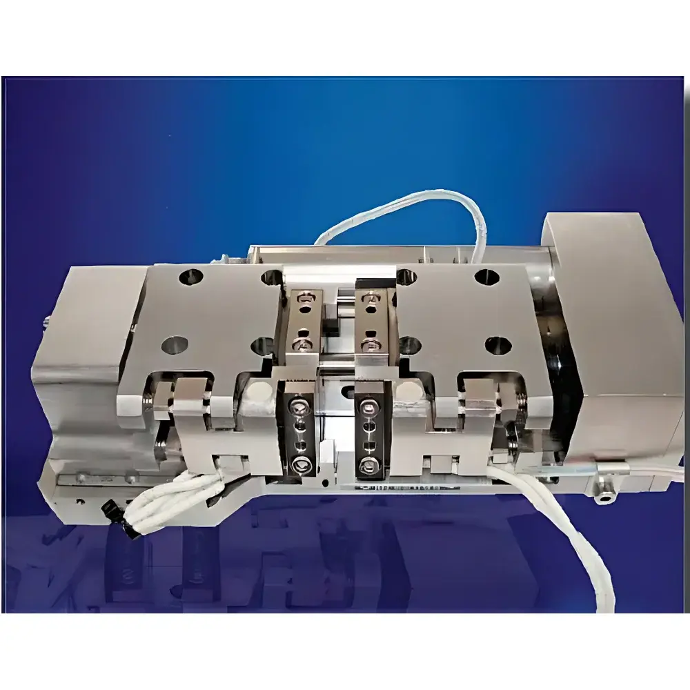
The Gatan MICROTEST 2000E is an engineered in-situ dynamic tensile and compression testing stage designed for integration within scanning electron microscopes (SEM) to enable real-time mechanical characterization at the microstructural level. Based on precision electromechanical actuation and high-stability load frame architecture, it operates on the principle of controlled uniaxial force application while maintaining full compatibility with high-resolution SEM imaging, energy-dispersive X-ray spectroscopy (EDS), and electron backscatter diffraction (EBSD). Its core functionality centers on synchronized mechanical loading and concurrent microstructural observation—enabling quantitative analysis of dislocation dynamics, grain rotation, twin nucleation, crack initiation, and strain localization under applied stress. The stage supports both static and dynamic test protocols—including constant-rate displacement, constant-load hold, low-frequency cyclic loading, and ramp-to-target-load sequences—making it suitable for fundamental metallurgical research, advanced materials development, and failure mechanism studies compliant with ASTM E8/E8M and ISO 6892-1 standards.
Key Features
- Maximum axial load capacity of 2000 N with integrated load cell (accuracy ±1% of full scale, resolution 0.1% FS)
- Linear extensometer with 3 µm resolution and 10 µm absolute accuracy for precise strain measurement
- Adjustable sample tilt angle up to 70°—optimized geometry for EBSD signal collection and pattern indexing
- Modular mechanical design compatible with standard SEM stubs; optional C1000XYX stage replacement for enhanced positional control
- Dual-mode operation: tension and compression, with programmable stroke range up to 10 mm
- Controlled displacement speed range from 0.033 mm/min to 0.4 mm/min (equivalent to 5.5 × 10⁻⁴ to 6.7 × 10⁻³ mm/s)
- Compact footprint: 196 × 96 × 53 mm (L × W × H); weight ~3.4 kg (2000ES), ~3.9 kg (2000EW)
- MTVideo synchronization module enables time-stamped video recording aligned with force/displacement data streams
Sample Compatibility & Compliance
The MICROTEST 2000E accommodates specimens up to 29 × 27 × 5 mm (L × W × H) for EBSD-optimized fixtures. It supports metallic alloys (e.g., Al, Ti, Fe-based systems), intermetallics, ceramics, and selected polymers—provided specimen geometry and conductivity meet SEM vacuum and imaging requirements. When equipped with the EH2000 heated fixture (available on the water-cooled MICROTEST 2000EW variant), in-situ thermal-mechanical testing is enabled up to 500 °C, supporting studies of recrystallization kinetics, phase transformation under stress, and thermally activated deformation mechanisms. All hardware and firmware comply with CE electromagnetic compatibility (EMC) directives and are designed for operation inside ultra-high vacuum (UHV) environments typical of field-emission SEMs. Mechanical calibration traceability follows ISO/IEC 17025 guidelines through accredited third-party verification.
Software & Data Management
The proprietary MICROTEST Control Software provides a deterministic real-time interface for test configuration, execution, and post-processing. It delivers live plotting of stress–strain curves with adjustable cursors, multi-scale zooming, and overlay capability for comparative analysis across multiple tests. Data export conforms to ASCII CSV and HDF5 formats for seamless integration with MATLAB, Python (NumPy/Pandas), and commercial finite element pre-processors. Audit trails—including user login timestamps, parameter changes, and hardware status logs—are maintained per GLP/GMP requirements. Optional FDA 21 CFR Part 11 compliance package includes electronic signatures, role-based access control, and immutable data archiving—suitable for regulated R&D environments.
Applications
- Crystallographic texture evolution during plastic deformation, quantified via time-resolved EBSD mapping
- In-situ observation of slip band formation, stacking fault propagation, and martensitic transformation in shape-memory alloys
- Micromechanical assessment of weld zones, additive-manufactured lattices, and thin-film/substrate interfaces
- Thermo-mechanical coupling studies using the EH2000 heating module—e.g., stress-assisted grain growth or dynamic recovery
- Microcrack nucleation and coalescence in brittle phases or composite reinforcements under monotonic or cyclic loading
- Validation of crystal plasticity finite element models (CPFEM) using experimentally derived orientation maps and local strain fields
FAQ
Is the MICROTEST 2000E compatible with all SEM platforms?
Yes, when used with standard SEM stub adapters; however, chamber depth, pole piece clearance, and detector positioning may require minor mechanical alignment—especially for EBSD-enabled configurations.
Can the system perform compression testing?
Yes—mechanical design supports bidirectional actuation; compression mode requires appropriate sample geometry and support fixtures to prevent buckling.
What is the minimum resolvable strain increment?
With the integrated linear extensometer, strain resolution is 3 µm over a 10 mm gauge length—equivalent to ~300 µε under ideal alignment conditions.
Does the system support automated test sequences?
Yes—scripted workflows allow batch execution of ramp-hold-relax cycles, load-controlled dwell steps, and conditional triggers based on real-time feedback signals.
Is vacuum compatibility verified?
All internal components are UHV-compatible (outgassing rate <1×10⁻⁹ mbar·L/s·cm²); non-metallic seals use Viton or Kalrez depending on temperature configuration.


