Hitachi AFM100 Series Multifunctional Scanning Probe Microscope
| Brand | Hitachi |
|---|---|
| Origin | Japan |
| Manufacturer | Hitachi High-Tech Corporation |
| Type | Atomic Force Microscope (AFM) |
| Model | AFM100 |
| Instrument Category | Materials-Grade AFM |
| Position Detection Noise | 0.03 nm |
| Maximum Sample Diameter | ≤35 mm |
| Maximum Sample Thickness | ≤10 mm |
| Sample Stage Travel Range | 5 mm |
Overview
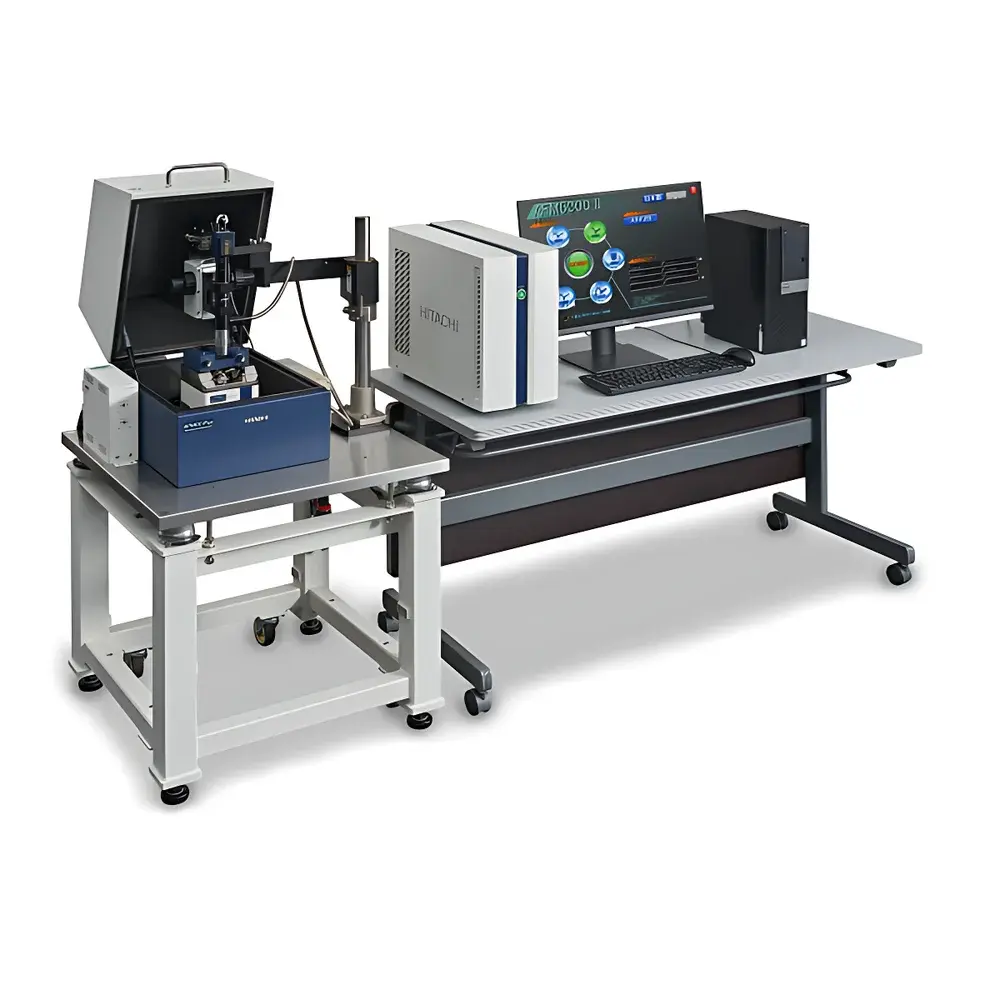
The Hitachi AFM100 Series is a multifunctional, materials-grade scanning probe microscope engineered for high-resolution surface topography and nanomechanical characterization in industrial R&D, quality control, and academic laboratories. Based on contact, tapping, and non-contact atomic force microscopy (AFM) modes, the system employs a laser beam deflection detection method with a quadrant photodiode to measure cantilever deflection with sub-angstrom sensitivity. Its low-position-detection-noise architecture (≤0.03 nm RMS in closed-loop operation) enables quantitative nanoscale metrology of surface roughness, step height, grain morphology, and local mechanical properties—including modulus mapping via force-distance spectroscopy—without requiring ultra-high-vacuum or conductive sample preparation. Designed as a turnkey platform for routine use, the AFM100 integrates robust mechanical stability, thermal drift compensation, and vibration-isolated optical path design to maintain measurement repeatability across extended acquisition sessions.
Key Features
- Pre-aligned, plug-and-play probe cartridge system ensures rapid, contamination-free cantilever exchange with minimal alignment recalibration.
- One-click automated measurement workflow—including auto-focus, auto-tune, scan parameter optimization, and real-time image processing—reduces operator dependency and training time.
- Integrated AFM marking function generates precise coordinate-based fiducial markers directly on the sample surface, enabling seamless correlative analysis with SEM and EDS systems using shared stage coordinates.
- Closed-loop piezoelectric scanner with 5 mm travel range provides large-area navigation while maintaining sub-nanometer positional fidelity and linearity correction via integrated capacitive feedback.
- Modular design supports optional upgrades including electrical mode (conductive AFM, Kelvin probe force microscopy), magnetic mode (MFM), and nanoindentation modules—all sharing the same control interface and data format.
- Compact footprint and ambient-air operation eliminate need for dedicated cleanroom infrastructure or vacuum pumping systems.
Sample Compatibility & Compliance
The AFM100 accommodates non-conductive, semi-conductive, and conductive solid samples up to 35 mm in diameter and 10 mm in thickness—including thin films, polymers, ceramics, metals, composites, and biological substrates (e.g., mica-supported proteins or dried cells). No sputter coating or conductive treatment is required for most imaging modes. The system complies with ISO/IEC 17025 calibration traceability requirements for dimensional metrology instruments when operated with certified reference standards (e.g., NIST-traceable grating samples). All firmware and software modules adhere to GLP-compliant audit trail protocols, supporting 21 CFR Part 11–aligned electronic signature and data integrity workflows where required for regulated environments.
Software & Data Management
Hitachi’s proprietary SPM Control Suite v4.x provides unified control of scanning, signal acquisition, real-time filtering, and multi-modal data fusion. Raw data is stored in vendor-neutral HDF5 format with embedded metadata (scan parameters, timestamp, environmental conditions, user ID), ensuring long-term archival compatibility and third-party analysis interoperability (e.g., with Gwyddion, MountainsSPIP, or Python-based SciPy pipelines). Batch processing scripts support automated roughness statistics (Sa, Sq, Sz per ISO 25178), power spectral density (PSD) analysis, and cross-sectional profiling. Software validation documentation—including IQ/OQ/PQ test protocols—is available upon request for laboratory accreditation purposes.
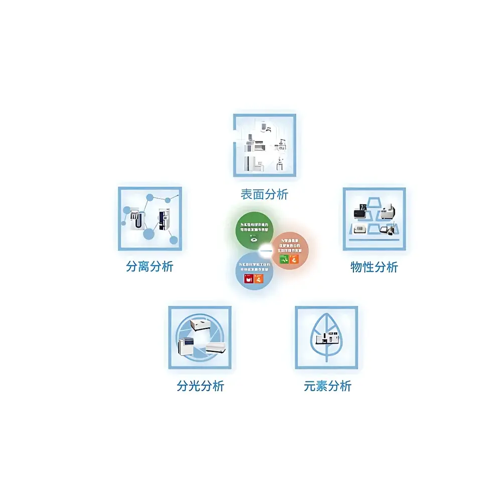
Applications
- Surface roughness quantification of optical coatings, semiconductor wafers, and medical device surfaces per ISO 4287 and ISO 25178 standards.
- Nanoscale defect identification and root-cause analysis in battery electrode layers, OLED encapsulation films, and MEMS packaging interfaces.
- Mechanical property mapping of polymer blends, hydrogels, and tissue-engineered scaffolds using force-volume and peak-force tapping modes.
- Correlative nanoscale structural–chemical–electrical analysis via registered AFM–SEM–EDS datasets for failure analysis in advanced packaging and heterogeneous integration.
- Teaching and training in nanoscience curricula, leveraging intuitive GUI, preconfigured experiment templates, and instructor-led remote session capabilities.
FAQ
Is the AFM100 compatible with standard commercial AFM probes?
Yes—the system accepts industry-standard rectangular and V-shaped cantilevers with nominal spring constants from 0.01 N/m to 40 N/m and resonance frequencies between 15 kHz and 300 kHz.
Can the AFM100 operate in liquid or controlled atmosphere environments?
The base configuration is optimized for ambient air operation; optional liquid cell and environmental chamber modules are available for in-situ electrochemical AFM and humidity-controlled measurements.
Does the system support automated tip qualification and wear monitoring?
Yes—integrated tip shape recognition algorithms analyze approach curves and topographic consistency across multiple scan lines to flag degradation before image artifacts occur.
What level of technical support and service coverage is provided outside Japan?
Hitachi High-Tech offers global service networks with local field application engineers, on-site preventive maintenance contracts, and remote diagnostics via secure TLS-encrypted connection.
Are raw data files exportable for third-party analysis without proprietary software dependencies?
All acquired data—including topography, error, amplitude, phase, and force curves—is exported in open HDF5 format with documented schema and SI-unit metadata, enabling full reproducibility in MATLAB, Python, or ImageJ/Fiji environments.


