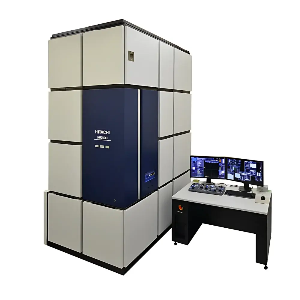
Hitachi HF5000 200 kV Spherical Aberration-Corrected Transmission Electron Microscope
| Brand | Hitachi |
|---|---|
| Origin | Japan |
| Manufacturer Type | Original Equipment Manufacturer (OEM) |
| Product Origin | Imported |
| Model | HF5000 |
| Accelerating Voltage | Up to 200 kV |
| Magnification | TEM (×200–×4,000,000), STEM (×20–×4,000,000) |
| HAADF-STEM Resolution | 0.78 Å |
| EDS Solid Angle | Up to 2.0 sr (dual-windowless silicon drift detectors) |
| Imaging Modes | TEM, STEM, SEM, Selected-Area Electron Diffraction (SAED), Convergent-Beam Electron Diffraction (CBED) |
Overview
The Hitachi HF5000 is a high-performance 200 kV spherical aberration-corrected transmission electron microscope engineered for atomic-resolution structural and compositional analysis across advanced materials science, semiconductor process development, catalysis research, and life sciences applications. At its core, the HF5000 employs a cold field-emission gun (CFEG) delivering exceptional beam coherence and current stability—critical for high signal-to-noise imaging and quantitative spectroscopy. Its integrated hexapole-based spherical aberration (Cs) corrector enables sub-angstrom resolution in both high-angle annular dark-field scanning transmission electron microscopy (HAADF-STEM) and conventional TEM imaging modes. With a verified HAADF-STEM resolution of 0.78 Å under standard operating conditions, the system supports direct visualization of light-element columns (e.g., oxygen, nitrogen) alongside heavy atoms in complex heterostructures, interfaces, and defect configurations.
Key Features
- Automated Cs correction workflow: Fully motorized, software-guided alignment eliminates manual tuning; achieves stable aberration correction within minutes without user intervention—optimized for shared-facility environments with high instrument utilization.
- Tri-modal imaging architecture: Seamless switching between TEM, STEM, and low-voltage SEM imaging on a single platform via reconfigurable detector geometry and beam path routing—enabling simultaneous acquisition of internal crystallinity (TEM/STEM) and surface topography (SEM) from identical sample regions.
- Dual windowless silicon drift detector (SDD) EDS system: Combined solid angle up to 2.0 sr ensures high X-ray collection efficiency; supports rapid, high-fidelity elemental mapping at nanometer spatial resolution with detection limits below 0.1 wt% for most elements (Z ≥ 5).
- Redesigned column and stage architecture: Enhanced mechanical rigidity and active vibration damping reduce thermal drift and acoustic perturbations; the ultra-stable specimen stage offers ±30° tilt range, 5-axis precision control, and sub-nanometer repeatability over extended acquisition periods.
- Forward-compatible platform design: Modular vacuum chamber interface and standardized electrical/data bus allow future integration of environmental stages (e.g., gas cell, heating/cooling holders), in situ biasing systems, or cathodoluminescence modules without hardware retrofits.
Sample Compatibility & Compliance
The HF5000 accommodates standard 3 mm TEM grids (including holey carbon, graphene oxide, and ultrathin SiN membranes), lamellae prepared by FIB-SEM, and bulk samples compatible with low-kV SEM mode (down to 1 kV). All operational parameters—including accelerating voltage, probe current, and detector gain—are traceable to NIST-traceable calibration standards. The system complies with ISO/IEC 17025 requirements for testing laboratories and supports audit-ready documentation for GLP and GMP-regulated workflows. Optional FDA 21 CFR Part 11-compliant software modules provide electronic signatures, secure user access tiers, and immutable audit trails for data integrity assurance.
Software & Data Management
Acquisition and analysis are managed through Hitachi’s unified EMWorks suite, featuring real-time image processing, automated crystallographic indexing (via CBED/SAED pattern matching), and machine-learning-assisted particle picking for cryo-EM workflows. Raw data are stored in open-standard formats (EMDB-compliant MRC, TIFF, and HDF5), enabling interoperability with third-party tools including DigitalMicrograph, HyperSpy, and Python-based scientific computing stacks. Integrated metadata tagging includes instrument configuration, calibration logs, and user-defined experimental annotations—ensuring full FAIR (Findable, Accessible, Interoperable, Reusable) data principles adherence.
Applications
- Atomic-scale characterization of catalyst nanoparticles, grain boundaries, and dislocation cores in metallurgical alloys and battery electrode materials.
- Interface engineering analysis in high-mobility semiconductor heterostructures (e.g., GaN-on-SiC, 2D van der Waals stacks).
- Structural validation of protein–ligand complexes and membrane protein assemblies using cryo-STEM tomography.
- In-line failure analysis of advanced logic nodes (sub-3 nm technology) including gate-all-around FETs and buried power rails.
- Quantitative phase mapping in multiphase geological specimens and fossil fuel-derived carbons via combined EDS/EELS spectral imaging.
FAQ
What vacuum level does the HF5000 maintain in the electron optical column?
The system achieves ultra-high vacuum (UHV) conditions of ≤1 × 10⁻⁸ Pa in the gun and column regions using a combination of ion pumps, non-evaporable getter (NEG) strips, and turbomolecular pumping—ensuring long-term CFEG stability and minimal contamination buildup.
Is the HAADF-STEM resolution of 0.78 Å guaranteed under all operating conditions?
This value represents the manufacturer-specified point resolution under optimal conditions: 200 kV acceleration, fully corrected Cs and Cc, <1 nm beam convergence angle, and vibration-isolated installation. Actual performance depends on site-specific infrastructure and sample preparation quality.
Can the HF5000 be upgraded to support in situ gas or liquid cell experiments?
Yes—the platform includes pre-engineered flange ports and electrical feedthroughs for retrofitting commercially available environmental TEM holders, subject to Hitachi’s certified installation and safety validation protocols.
Does the dual-EDS configuration support spectral deconvolution of overlapping peaks (e.g., S Kα and Pb Mα)?
Yes—EMWorks includes proprietary peak-fitting algorithms based on physical detector response modeling and multi-detector coincidence filtering, significantly improving quantification accuracy for spectrally congested regions.


