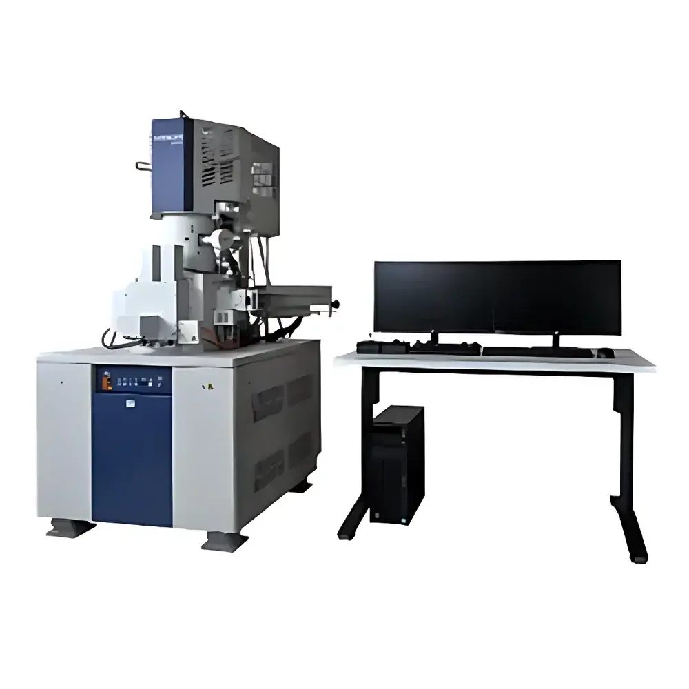
Hitachi SU8700 Schottky Field-Emission Scanning Electron Microscope
| Brand | Hitachi |
|---|---|
| Origin | Japan |
| Manufacturer | Hitachi High-Tech Corporation |
| Type | Floor-standing SEM |
| Electron Source | Schottky field-emission gun |
| Secondary Electron Resolution | 0.6 nm @ 15 kV, 0.8 nm @ 1 kV, 0.9 nm @ 0.3 kV |
| Magnification Range | 20× – 2,000,000× |
| Accelerating Voltage | 0.1–30 kV (standard mode) |
| Maximum Image Size (optional) | 40,960 × 30,720 pixels |
| Simultaneous Signal Channels | Up to 6 detectors |
| EDS Working Distance Optimization | Short WD configuration enabled via optimized chamber geometry |
Overview
The Hitachi SU8700 is a high-performance floor-standing Schottky field-emission scanning electron microscope (FE-SEM) engineered for nanoscale imaging, compositional analysis, and structural characterization across advanced materials science, semiconductor R&D, life sciences, and industrial quality control. Built upon Hitachi’s decades-long heritage in electron optics, the SU8700 integrates a thermally stable Schottky field-emission electron source with an ultra-rigid column architecture, enabling exceptional beam coherence, long-term current stability (>24 h drift < 0.5 nm), and sub-nanometer resolution at low accelerating voltages. Its optical design supports both high-resolution surface topography imaging (via in-lens SE detection) and high-sensitivity backscattered electron (BSE) contrast—though BSE spatial resolution is not specified as a standalone metric due to signal-dependent detector geometry and material interaction effects. The system operates under high vacuum (≤1 × 10⁻⁴ Pa) and features active vibration isolation, electromagnetic shielding, and temperature-stabilized lens coils to ensure measurement reproducibility in demanding laboratory environments.
Key Features
- Sub-nanometer secondary electron resolution: 0.6 nm at 15 kV, 0.8 nm at 1 kV, and 0.9 nm at 0.3 kV—enabling reliable imaging of beam-sensitive biological specimens, ultrathin films, and low-Z nanostructures without excessive charging or damage.
- Wide accelerating voltage range (0.1–30 kV) with stepless control, supporting both low-voltage surface-sensitive imaging and high-penetration microstructural analysis in conductive and semi-conductive samples.
- Optimized specimen chamber geometry enabling short working distance (WD) operation down to 3 mm for energy-dispersive X-ray spectroscopy (EDS), improving spatial resolution of elemental mapping by up to 40% compared to conventional configurations at equivalent kV.
- Simultaneous acquisition from up to six independent signal channels—including in-lens SE, through-the-lens BSE, STEM-in-SEM, and multiple segmented solid-state BSE detectors—allowing correlative interpretation of topography, crystallography, atomic number contrast, and phase distribution within a single scan.
- Ultra-high-definition imaging capability: optional 40,960 × 30,720 pixel frame size (1.25 billion pixels per image), representing a 64× increase over prior-generation Hitachi FE-SEMs—ideal for automated defect review, large-area metrology, and statistical grain/phase analysis.
Sample Compatibility & Compliance
The SU8700 accommodates standard 3-inch (76 mm) and 4-inch (100 mm) diameter wafers, bulk metal/ceramic coupons (up to 80 mm height), and TEM grid-mounted biological sections. Optional stage configurations support tilt (±90°), rotation (360°), and heating/cooling (–180°C to +1000°C). All vacuum interlocks, emission current monitoring, and high-voltage safety protocols comply with IEC 61010-1:2010 and JIS C 61010-1. For regulated environments, the system supports audit-trail-enabled operation when integrated with compliant LIMS or ELN platforms; full traceability of acquisition parameters, detector settings, and calibration logs meets GLP and GMP documentation requirements per FDA 21 CFR Part 11 when used with validated software modules.
Software & Data Management
Control and analysis are executed via Hitachi’s proprietary “EM Flow Creator” platform—a modular, scriptable environment supporting both GUI-driven workflows and Python-based automation. Predefined templates enable one-click alignment, focus/stigmation, and contrast optimization. Batch acquisition routines can be scheduled across multiple samples, with real-time metadata tagging (including stage position, kV, WD, dwell time, and detector gain). Raw data is stored in standardized TIFF/OME-TIFF formats with embedded EXIF-like metadata conforming to the Open Microscopy Environment (OME) schema. Integration with third-party tools—including Thermo Fisher Velox, Oxford AZtec, and Bruker Esprit—is achieved via documented APIs and HDF5 export options. All user actions, parameter changes, and software updates are logged with timestamps and operator IDs for audit readiness.
Applications
- Semiconductor process development: Critical dimension (CD) metrology on FinFETs, EUV photoresist line-edge roughness (LER) quantification, and buried interface inspection using low-kV SE imaging.
- Advanced battery materials: In situ and ex situ observation of cathode cracking, SEI layer morphology, and Li dendrite growth—enabled by variable-pressure and low-dose imaging modes.
- Metallurgy & ceramics: Grain boundary mapping via EBSD integration, phase identification using EDS spectral deconvolution, and porosity quantification in sintered components.
- Life sciences: Cryo-SEM preparation workflows for hydrated tissues, collagen fibril periodicity analysis, and nanoparticle-cell interaction studies under charge-compensated low-kV conditions.
- Failure analysis: Cross-sectional imaging of solder joint voids, delamination in multilayer PCBs, and electromigration-induced voiding in Cu interconnects.
FAQ
What vacuum level is maintained in the specimen chamber during operation?
The chamber achieves and sustains ≤1 × 10⁻⁴ Pa under standard operating conditions, with turbo-molecular pumping backed by a dry scroll pump. Vacuum integrity is continuously monitored via Bayard-Alpert and cold cathode gauges.
Is the SU8700 compatible with EBSD detectors from third-party vendors?
Yes—the system provides mechanical, electrical, and software interfaces compliant with HKL Channel 5, EDAX TEAM, and Oxford Symmetry EBSD standards, including synchronized stage positioning and pattern indexing triggers.
Can the 40,960 × 30,720 pixel mode be used for real-time navigation?
No—this ultra-high-resolution mode is acquisition-only and requires offline stitching or region-of-interest (ROI) targeting via lower-resolution survey images. Navigation remains optimized at ≤4,096 × 3,072 pixels for responsiveness.
Does the SU8700 support automated particle analysis out-of-the-box?
Basic particle detection and sizing are available via built-in “Particle Analysis” module; full ASTM E1245-compliant statistics require optional “Automated Particle Characterization Suite” with customizable thresholding, shape factor libraries, and ISO 13322-2 reporting templates.
How is beam current stability ensured during extended EDS mapping sessions?
The Schottky emitter incorporates real-time filament temperature feedback and emission current regulation circuitry, maintaining beam current variation within ±0.8% over 8-hour continuous operation—verified per ISO 16700 Annex B protocols.


