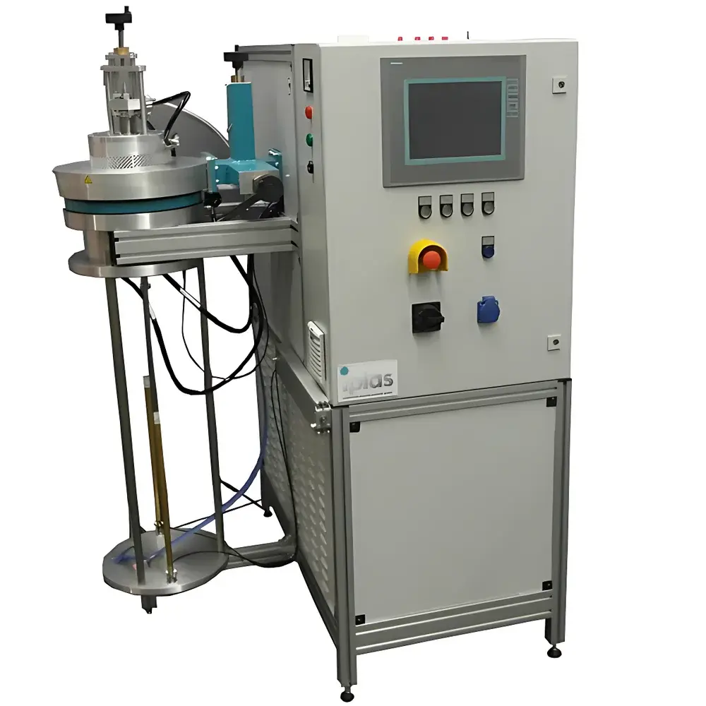
iplas CYRANNUS® Microwave Plasma Chemical Vapor Deposition System
| Brand | iplas |
|---|---|
| Origin | Germany |
| Model | CYRANNUS® |
| Operating Pressure Range | 10 mbar to atmospheric pressure |
| Plasma Generation Method | External multi-electrode microwave excitation (2.45 GHz or 915 MHz) |
| Substrate Compatibility | Up to 300 mm diameter planar or curved substrates |
| Compatible Precursor Gases | CH₄/H₂/O₂/Ar/He/N₂ (inert and reactive) |
| Deposited Materials | Single-crystal diamond, polycrystalline diamond, nanocrystalline diamond, DLC, Al₂O₃, c-BN |
| Plasma Stability | High reproducibility under dynamic gas flow, pressure, and voltage fluctuations |
| Safety Compliance | Fully shielded microwave cavity |
Overview
The iplas CYRANNUS® Microwave Plasma Chemical Vapor Deposition (MPCVD) System is an engineered platform for high-fidelity synthesis of wide-bandgap semiconductors and ultra-hard functional thin films. Unlike conventional RF or DC plasma CVD systems, the CYRANNUS® architecture employs externally coupled, multi-electrode microwave excitation—operating at either 2.45 GHz or 915 MHz—to generate a spatially confined, highly stable plasma ball directly within the process chamber. This configuration avoids internal electrodes, eliminating metallic contamination and enabling ultra-pure growth environments essential for electronic-grade single-crystal diamond (SCD) and optoelectronic-quality Al₂O₃ or cubic boron nitride (c-BN). The system operates across a broad pressure range—from 10 mbar up to ambient pressure—without plasma collapse or mode-hopping, a critical advantage over resonant-cavity-based MPCVD tools. Its plasma physics is grounded in non-equilibrium kinetics: electron temperatures (Te ≈ 1–3 eV) significantly exceed ion and neutral gas temperatures (Ti, Tg < 1500 K), permitting substrate heating control independent of plasma power. This enables low-thermal-budget crystallization of metastable phases while sustaining high precursor dissociation efficiency.
Key Features
- Electrode-free plasma generation: No internal electrodes or dielectric windows inside the deposition chamber—eliminating sputtering-induced contamination and extending maintenance intervals.
- Center-localized plasma confinement: External magnetic field integration allows precise spatial control of the plasma volume (diameters: 70–400 mm), minimizing wall interaction and preserving stoichiometric fidelity during film growth.
- Dynamic stability under process drift: Maintains consistent plasma impedance and electron density despite ±15% variation in gas flow rate, ±50 mbar pressure deviation, or ±5% microwave power fluctuation—ensuring uninterrupted monolayer-by-monolayer epitaxy.
- Modular microwave source compatibility: Supports scalable power inputs (1–30 kW) and frequency options (2.45 GHz for lab-scale precision; 915 MHz for industrial throughput), with standardized waveguide interfaces per IEC 60158-2.
- Full radiation safety compliance: Integrated Faraday shielding, dual-interlocked access doors, and real-time microwave leakage monitoring (<1 mW/cm² at 5 cm) conform to EN 50147-1 and ICNIRP occupational exposure limits.
- Thermal management architecture: Water-cooled chamber walls and programmable substrate heater (up to 1200 °C, ±0.5 °C stability) enable precise control of surface reaction kinetics without bulk overheating.
Sample Compatibility & Compliance
The CYRANNUS® system accommodates both planar wafers (Si, SiC, Ir, Mo, quartz) and irregular geometries—including spherical particles and micro-machined 3D structures—for conformal hard-coating applications. It supports heterogeneous nucleation on foreign substrates and homoepitaxial growth on diamond seeds (type Ib, IIa). All hardware components meet ISO 14644-1 Class 5 cleanroom compatibility standards when integrated with laminar-flow purge modules. Process protocols are fully traceable and audit-ready for GLP/GMP environments: temperature, pressure, gas flows, microwave forward/reflected power, and optical emission spectroscopy (OES) signals are timestamped and stored with 100 ms resolution. Optional OES integration supports real-time endpoint detection per ASTM E1782–21 for layer-thickness control.
Software & Data Management
Control is executed via iplas’ proprietary PlasmaSync™ software suite—a deterministic real-time OS (VxWorks-based) with deterministic loop timing (<10 ms). The interface provides full recipe management (IEC 62591-compliant), interlock logic configuration, and automated calibration routines for mass flow controllers and pressure transducers. All operational data—including spectral snapshots from optional UV-VIS-NIR OES—are exported in HDF5 format with embedded metadata compliant with FAIR principles. Audit trails satisfy FDA 21 CFR Part 11 requirements, including electronic signatures, role-based access control, and immutable log archiving. Remote diagnostics and firmware updates are supported via TLS 1.3-secured Ethernet connection—no cloud dependency.
Applications
- Growth of >10 carat, VVS1-grade gemstone-quality single-crystal diamond for jewelry and quantum sensing platforms.
- Homoepitaxial SCD layers (>500 µm thick) for high-power RF electronics and neutron detectors (ASTM F2563–20).
- High-orientation diamond films on Si or Mo substrates for thermal interface materials in GaN HEMTs.
- Al₂O₃ dielectric layers for MEMS capacitors and passivation in harsh-environment sensors (ISO 20482–22).
- c-BN synthesis on TiN-coated tooling inserts for ultra-precision machining of hardened steels (ISO 513–21).
- Nanocrystalline diamond and DLC coatings on biomedical implants (ISO 14286–23) and tribological surfaces.
FAQ
What distinguishes CYRANNUS® plasma from conventional resonant-cavity MPCVD?
The external multi-electrode coupling eliminates standing-wave nodes and cavity tuning dependencies—enabling stable plasma ignition and maintenance across the full 10 mbar–1000 mbar range without mechanical tuners or auto-matching networks.
Can the system deposit on non-planar substrates?
Yes. The spatially uniform plasma distribution and absence of line-of-sight constraints allow conformal deposition on spherical, conical, or micro-structured surfaces—validated for 1–5 mm diameter diamond grit and ceramic microspheres.
Is process validation support available for regulated industries?
iplas provides IQ/OQ documentation packages aligned with ISO 9001:2015 and ASTM E2500–13, including as-built schematics, calibration certificates, and traceable test reports for pressure, temperature, and gas delivery subsystems.
How is plasma uniformity quantified and maintained?
Uniformity is verified using spatially resolved OES intensity mapping (±3% RMS deviation across 200 mm diameter) and confirmed via Raman mapping of deposited diamond films (FWHM < 3.5 cm⁻¹ at 1332 cm⁻¹ peak).
What vacuum specifications are required for base operation?
A turbomolecular pumping station capable of ≤5×10⁻⁷ mbar base pressure is recommended prior to process gas introduction; however, the system does not require ultra-high vacuum for routine diamond growth due to its robust plasma stabilization design.


