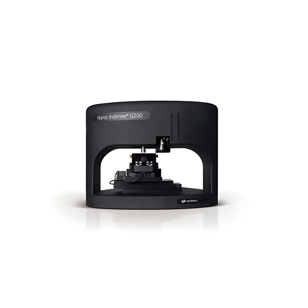
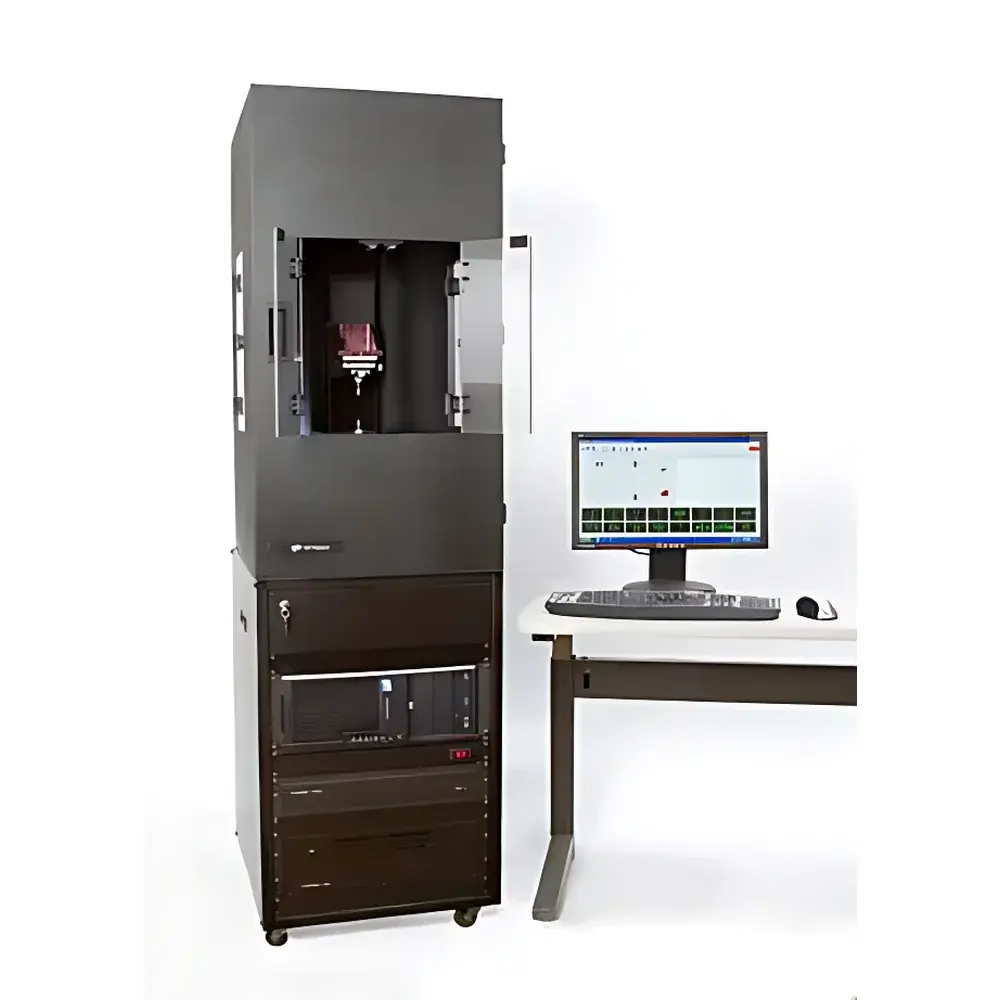
Keysight G200 / InSEM / iMicro / iNano Nanoindentation and Scratch Testing System
| Brand | Keysight |
|---|---|
| Origin | USA |
| Model | G200 / InSEM / iMicro / iNano |
| Instrument Type | Integrated Nanoindentation and Scratch Tester |
| Indenter Types | Dozens of interchangeable tips (Berkovich, Cube-corner, Spherical, Conical, etc.) |
| Compliance | ASTM E2546, ISO 14577, USP <1062>, GB/T 22458–2008, GB/T 25898–2010 |
| Measurement Principle | Continuous Stiffness Measurement (CSM), Dynamic Contact Depth Control, Load-Displacement Feedback Loop |
Overview
The Keysight G200 / InSEM / iMicro / iNano series represents a family of high-precision, modular nanoindentation and scratch testing systems engineered for quantitative mechanical characterization at the micro- and nanoscale. These instruments operate on the fundamental principles of depth-sensing indentation mechanics, where controlled force is applied via a calibrated diamond indenter while continuously monitoring displacement with sub-nanometer resolution. The core measurement methodology—Continuous Stiffness Measurement (CSM)—enables real-time determination of contact stiffness during loading, allowing for accurate calculation of reduced modulus and hardness without reliance on post-test unloading curve fitting alone. All models support both static and dynamic indentation protocols, including quasi-static creep, strain-rate jump, and harmonic oscillation modes. The InSEM variant integrates directly into scanning electron microscopes (SEMs) for in situ mechanical testing under high-resolution imaging; iMicro targets micron-scale features with enhanced load range (up to 10 N); iNano delivers ultra-high resolution for thin films and 2D materials (sub-10 nN force resolution, <0.05 nm depth resolution); and the flagship G200 platform provides broad versatility across research and industrial QA/QC environments.
Key Features
- Modular architecture enabling seamless configuration as standalone nanoindenter (G200), SEM-integrated in situ tester (InSEM), micro-scale mechanical tester (iMicro), or ultra-high-resolution nanomechanical analyzer (iNano)
- Patented electromagnetic transducer with active damping and closed-loop force/displacement control ensuring <0.5% load linearity and <0.1 nm displacement noise floor
- CSM technology compliant with ISO 14577-1:2015 and ASTM E2546–18 for modulus/hardness mapping, validated against NIST-traceable reference materials
- Automated tip calibration using fused silica and sapphire standards with integrated thermal drift compensation
- Multi-axis motorized stage with ±10 µm positioning repeatability and programmable Z-axis approach velocity (1 nm/s to 10 µm/s)
- Real-time acoustic emission detection for fracture onset identification during scratch and indentation tests
Sample Compatibility & Compliance
The system accommodates diverse sample geometries—including wafers up to 300 mm, polished cross-sections, freestanding membranes, MEMS devices, biological tissue sections, and irregularly shaped bulk specimens—via customizable holders and vacuum chucks. Environmental options include heated/cooled stages (−100 °C to 600 °C), humidity-controlled chambers, and liquid cell modules for hydrated testing. All configurations meet GLP/GMP documentation requirements with full audit trail functionality. Data acquisition and reporting conform to FDA 21 CFR Part 11 for electronic records and signatures. Test methods align with international standards: ISO 14577 (metallic and non-metallic materials), ASTM E2546 (polymer nanocomposites), USP (pharmaceutical coatings), and Chinese national standards GB/T 22458–2008 and GB/T 25898–2010, which explicitly incorporate Keysight’s CSM methodology.
Software & Data Management
TriboScan™ software provides unified control across all platforms, supporting script-based automation (Python API), multi-parameter mapping (hardness, modulus, creep, dissipation), and statistical analysis (Weibull distribution, spatial autocorrelation). Raw load-displacement data are stored in HDF5 format with embedded metadata (timestamp, operator ID, calibration history, environmental conditions). Export options include CSV, MATLAB .mat, and MIF (Materials Information Format) for interoperability with Thermo Scientific Avizo, MATLAB, and Python-based machine learning pipelines. Secure user roles (admin/operator/analyst), electronic signature workflows, and encrypted database backups ensure regulatory compliance in pharmaceutical, aerospace, and medical device development.
Applications
These systems serve as primary tools in advanced materials R&D and production validation. Typical use cases include: evaluating interfacial adhesion strength of ALD-grown dielectric layers on Si substrates; quantifying size-dependent modulus gradients in gradient-index metamaterials; assessing time-dependent viscoelastic recovery in hydrogel-based biosensors; measuring fracture toughness of thermal barrier coatings under simulated turbine operating temperatures; characterizing wear resistance of DLC-coated orthopedic implants; and validating mechanical integrity of printed electronics after thermal cycling. Cross-disciplinary applications span semiconductor process development, battery electrode coating optimization, additive manufacturing quality assurance, biomaterial scaffold design, and nuclear fuel cladding performance modeling.
FAQ
What distinguishes CSM from conventional nanoindentation methods?
CSM superimposes a small oscillatory load on the primary ramp, enabling continuous stiffness measurement throughout loading—critical for capturing property gradients in functionally graded materials and avoiding artifacts from pile-up or sink-in.
Can the InSEM system operate inside any SEM chamber?
Yes, provided the SEM offers sufficient chamber clearance (≥120 mm vertical space), compatible vacuum interface (KF40 or CF63 flange), and electrical feedthroughs for signal transmission and piezo control.
Is tip geometry verification required before each test series?
While automated tip shape reconstruction is performed daily using standard reference samples, tip certification per ASTM E2546 mandates periodic verification using certified Berkovich tips traceable to NIST SRM 2241.
How is thermal drift compensated during long-duration creep experiments?
A dual-sensor architecture monitors both indenter displacement relative to the sample surface and thermal expansion of the load frame, feeding real-time corrections into the PID loop with <0.02 nm/min drift suppression.
Does the system support third-party SPM integration?
Yes—via standardized SPI interface and vendor-neutral driver libraries, enabling synchronized operation with AFM, STM, and conductive-AFM modules for correlative nanomechanical-electrical mapping.


