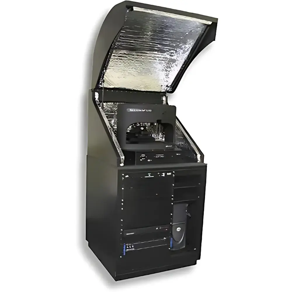
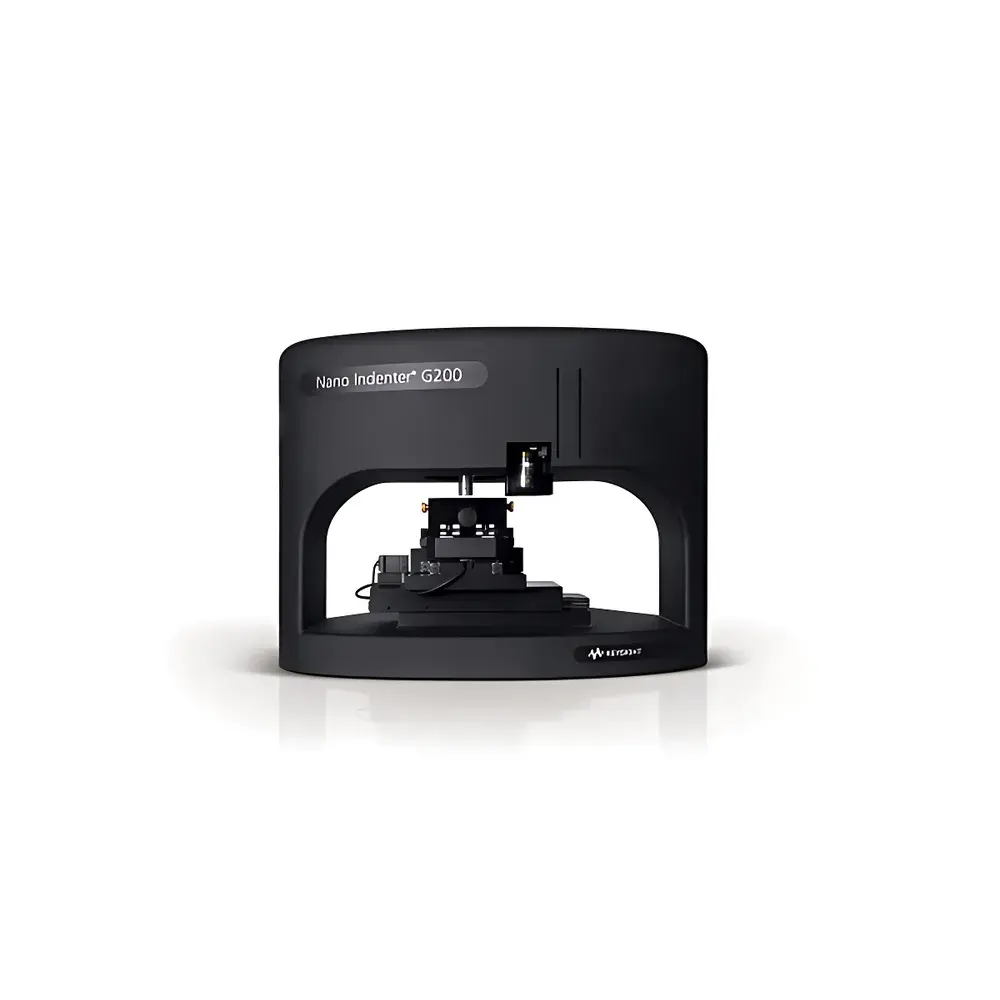
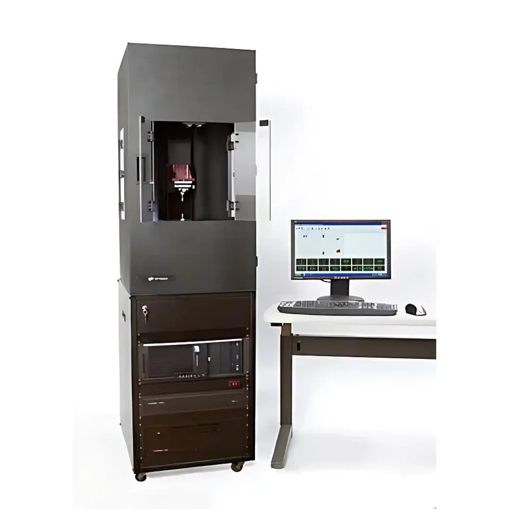
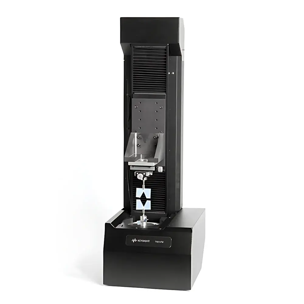
Keysight K-T G200/T150/iNano/InSitu Nanoindentation and Scratch Testing System
| Brand | Keysight |
|---|---|
| Origin | USA |
| Model Series | G200, T150, iNano, InSitu |
| Instrument Type | Nanoindentation and Scratch Tester |
| Maximum Load Capacity | 10 N |
| Load Resolution | <1 nN |
| Displacement Resolution | <0.02 nm |
| Indenter Types | Berkovich, Cube-Corner, Vickers, Spherical (radius down to 1 µm) |
| Standard Test Load | 500 mN |
| Core Technology | Continuous Stiffness Measurement (CSM), In-Situ Nanomechanical Testing, High-Resolution Scanning Probe Imaging |
| Compliance | ASTM E2546, ISO 14577, GB/T 22458 (Chinese National Standard incorporating K-T CSM patent) |
Overview
The Keysight K-T G200, T150, iNano, and InSitu series represent the industry benchmark in quantitative nanomechanical characterization. Engineered for precision and traceability, these systems implement a hybrid electrostatic–capacitive transduction architecture optimized for ultra-low-noise force and displacement sensing. At their core lies the patented Continuous Stiffness Measurement (CSM) technique—originally developed by the predecessor Agilent Nanomechanics Division, acquired by Keysight in April 2018. CSM enables real-time, depth-resolved determination of reduced modulus (Er) and hardness (H) during indentation, without requiring unloading segment analysis. This principle is codified in ASTM E2546, ISO 14577, and China’s GB/T 22458, where K-T’s CSM methodology serves as the technical foundation for standardized nanoindentation testing. The platform supports both static and dynamic nanomechanical protocols—including high-frequency oscillatory loading (up to 200 Hz), creep relaxation, and strain-rate jump experiments—making it suitable for viscoelastic polymers, thin-film coatings, biomaterials, and next-generation semiconductor interconnects.
Key Features
- Sub-nanonewton load resolution (<1 nN) and sub-0.02 nm displacement resolution, enabling reliable mechanical property mapping at sub-10 nm indentation depths.
- Dual-mode actuation architecture: electrostatic positioning for coarse approach and capacitive feedback-controlled piezoelectric actuation for fine control—ensuring stability under thermal drift and environmental vibration.
- Integrated scanning probe imaging capability with lateral resolution down to 10 nm, supporting topography-guided indentation and correlative nano-mechanical + morphological analysis.
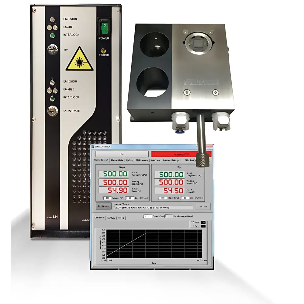
- In-situ testing variants (e.g., InSitu series) feature modular vacuum or inert-gas chambers, integrated heating/cooling stages (−120 °C to 800 °C), and electrical biasing interfaces for electromechanical coupling studies.
- Modular indenter library: interchangeable Berkovich, cube-corner, spherical (1–100 µm radius), and custom geometry tips—calibrated per ISO 14577 Annex B using fused silica and sapphire reference standards.
Sample Compatibility & Compliance
The system accommodates rigid and compliant substrates ranging from single-crystal silicon wafers to soft hydrogels (modulus range: 0.1 MPa to 1000 GPa). Sample mounting is compatible with standard SEM stubs, TEM grids, and custom fixtures for tensile-strained films or microcantilevers. All measurement workflows comply with Good Laboratory Practice (GLP) and Good Manufacturing Practice (GMP) requirements, including full audit trails, electronic signatures, and 21 CFR Part 11–compliant software validation packages. Data export formats include ASTM E1392-compliant XML, HDF5, and CSV with metadata embedding (test parameters, calibration history, environmental logs).
Software & Data Management
Keysight NanoTest Control Software v6.x provides a deterministic, scriptable environment built on a real-time Linux kernel. It supports automated grid-based mapping (up to 10,000 points), multi-cycle fatigue testing, and batch processing with statistical post-analysis (Weibull modulus, coefficient of variation, spatial autocorrelation). Raw force–displacement data are stored with hardware-timestamped metadata; all analysis modules—including Oliver–Pharr, Doerner–Nix, and time-dependent viscoelastic models—are open-source validated and user-modifiable. Software validation documentation (IQ/OQ/PQ protocols) and cybersecurity compliance reports (IEC 62443-3-3) are available upon request.
Applications
- Thin-film adhesion quantification via progressive-load scratch testing with acoustic emission monitoring and post-test SEM/FIB cross-section correlation.
- Depth-dependent modulus profiling across graded oxide layers in advanced gate stacks (e.g., HfO2/SiO2/Si).
- Mechanical heterogeneity mapping in battery electrode composites (NMC cathodes, silicon anodes) under controlled humidity and temperature.
- Creep compliance and stress relaxation modeling of medical hydrogels (e.g., PEGDA, hyaluronic acid derivatives) relevant to FDA 510(k) submissions.
- In-situ nanoindentation inside SEM chambers for real-time dislocation nucleation observation in metallic glass ribbons.
FAQ
What distinguishes CSM from conventional quasi-static nanoindentation?
CSM superimposes a small oscillatory load (typically ±1–5% of peak load) at a defined frequency during indentation. By continuously analyzing the phase lag and amplitude ratio between force and displacement, it calculates contact stiffness—and thus Er and H—in real time, eliminating reliance on idealized unloading curves.
Is the system compatible with third-party environmental stages?
Yes. The mechanical interface conforms to ISO 80000-4 mounting standards; Keysight provides API-level integration support for commercial heating, cooling, and electrochemical cells.
How is tip geometry calibrated and certified?
Each indenter undergoes SEM-based apex radius verification and area function calibration against NIST-traceable fused silica and sapphire standards. Calibration certificates include uncertainty budgets per ISO/IEC 17025.
Can the system perform quantitative scratch adhesion testing per ISO 20502?
Yes. The T150 and InSitu platforms meet ISO 20502 requirements for critical load determination, friction coefficient tracking, and residual groove profilometry using integrated white-light interferometry.
What level of software validation support is provided for regulated industries?
Keysight delivers full GxP validation packages—including risk assessments, URS, FRS, test scripts, and summary reports—aligned with FDA, EMA, and NMPA expectations for analytical instrument qualification.


