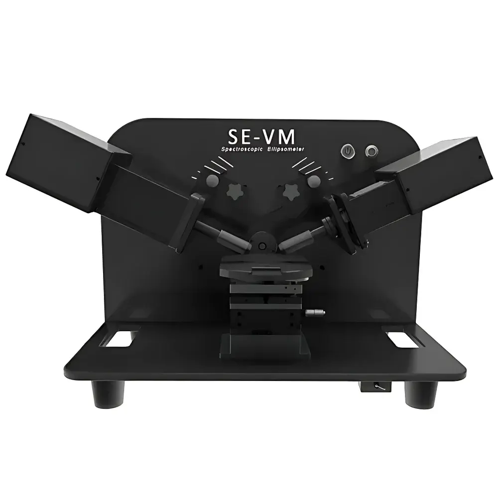
KJ GROUP SE-VM High-Precision Spectroscopic Ellipsometer
| Brand | KJ GROUP |
|---|---|
| Origin | Liaoning, China |
| Manufacturer Type | Authorized Distributor |
| Origin Category | Domestic (China) |
| Model | SE-VM |
| Pricing | Available Upon Request |
| Light Source Range | 380–1000 nm (expandable to 210–1650 nm) |
| Measurement Parameters | Ψ/Δ, n/k/s, R/T spectra |
| Acquisition Speed | 0.5–5 s per spectrum |
| Repeatability | ±0.01 nm |
| Spot Size | 2–3 mm (standard), 200 µm (micro-spot option) |
| Angle of Incidence | 55°–75° (5° increments), 90° |
| Angle Adjustment | Manual goniometer |
| Focusing Method | Manual focus |
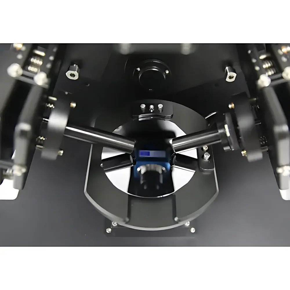
| Sample Max Diameter | 180 mm |
| Mapping Capability | Not supported |
| Optional Accessories | Temperature-controlled stage, Transmission adsorption module, Vacuum pump, Mapping expansion kit |
Overview
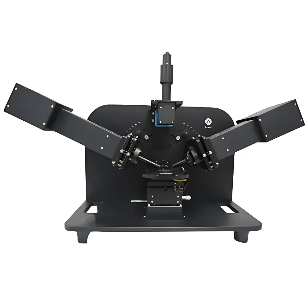
The KJ GROUP SE-VM Spectroscopic Ellipsometer is an engineered solution for non-destructive, high-precision optical characterization of thin films and nanostructured surfaces. Based on the fundamental principles of spectroscopic ellipsometry—measuring the change in polarization state (Ψ and Δ) of light reflected from a sample surface—the SE-VM delivers quantitative determination of complex refractive index (n + ik), film thickness, interfacial roughness, and geometric profile parameters across the visible to near-infrared spectral range (380–1000 nm, extendable to 210–1650 nm). Its design emphasizes metrological robustness and configurability for R&D laboratories and production environments where rapid, repeatable optical metrology is critical—particularly in optical coating development, semiconductor process monitoring, photonic device fabrication, and advanced material research.
Key Features
- High-stability broadband composite light source with spectral coverage from 380 nm to 1000 nm, compatible with optional UV–NIR extension modules for extended material characterization.
- Phase-compensated rotating compensator (PCRSA) configuration enabling high-fidelity, high-speed acquisition of Ψ/Δ spectra with minimal instrumental artifacts.
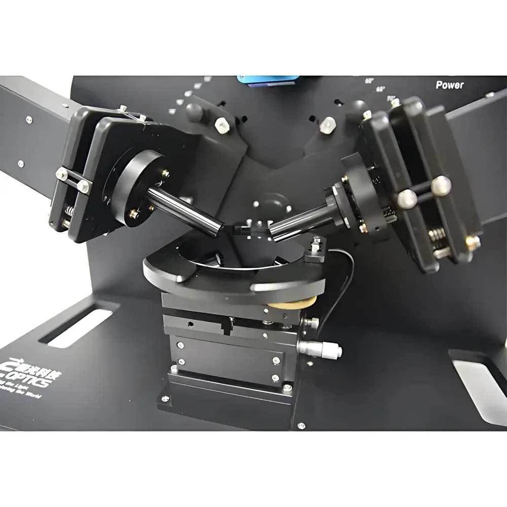
- Manually adjustable incidence angle goniometer supporting discrete angles from 55° to 75° in 5° steps, plus normal incidence (90°), facilitating multi-angle modeling for anisotropic or multilayer systems.
- Dual-spot optical path: standard 2–3 mm spot for macro-scale uniformity assessment and optional 200 µm micro-spot for localized analysis of patterned substrates or heterogeneous thin-film regions.
- Integrated visual leveling system with real-time camera feedback ensures precise sample alignment and minimizes tilt-induced measurement error—a critical factor for sub-nanometer thickness resolution.
- Modular architecture supports field-upgradable functionality, including temperature-controlled stages (for in-situ thermal optical property studies), vacuum-compatible configurations, and transmission-mode accessories for transparent substrate analysis.
Sample Compatibility & Compliance
The SE-VM accommodates flat, rigid substrates up to 180 mm in diameter, including silicon wafers, glass slides, fused silica, sapphire, and metal-coated optics. It is optimized for isotropic and weakly anisotropic dielectric, semiconductor, and metallic thin films—ranging from monolayer 2D materials to multilayer interference stacks exceeding 10 layers. While not certified for GLP/GMP environments out-of-the-box, its data output structure (ASCII-based spectral datasets, metadata-rich headers) conforms to ASTM E2581–22 and ISO 15022 standards for ellipsometric data reporting. When integrated with validated SOPs and external audit trails, the system supports traceable metrology workflows aligned with ISO/IEC 17025 requirements.
Software & Data Management
The SE-VM operates with KJ GROUP’s proprietary ellipsometry analysis suite, featuring a model-driven fitting engine with over 300 preloaded optical constants for metals, oxides, nitrides, polymers, and emerging optoelectronic materials (e.g., perovskites, TMDs). Users may construct custom multilayer, graded-index, or effective-medium models using intuitive graphical interfaces. The software implements Levenberg–Marquardt and global optimization algorithms, with uncertainty estimation via covariance matrix analysis. Raw and processed data export formats include CSV, TXT, and JPK-compatible .spm for cross-platform interoperability. Audit trail logging (user actions, parameter changes, fit residuals) is enabled for internal quality documentation; full 21 CFR Part 11 compliance requires integration with third-party electronic lab notebook (ELN) systems.
Applications
- Real-time monitoring of PVD, CVD, ALD, and spin-coated film growth for thickness and optical constant calibration (tooling factor derivation).
- Quantitative analysis of anti-reflective, high-reflection, and dichroic coatings—supporting ISO 9211–3 verification protocols.
- Characterization of porous low-k dielectrics, graphene oxide layers, and quantum dot monolayers where conventional reflectometry lacks sensitivity.
- Interfacial analysis of buried interfaces (e.g., SiO₂/Si, ITO/glass) without requiring physical sectioning or destructive TEM preparation.
- Support for optical constants database curation in academic and industrial optical design workflows (e.g., integration with CODE V, Zemax, or RCWA solvers).
FAQ
What spectral range does the standard SE-VM configuration cover?
The base system operates from 380 nm to 1000 nm. Extended-range versions supporting 210–1650 nm are available as factory-configured options with UV-enhanced optics and InGaAs/NIR detectors.
Is automated angle scanning supported?
No—the SE-VM uses a manual goniometer for incidence angle selection. Automated angle control is not included but can be implemented via third-party motorized stages interfaced through TTL/RS-232.
Can the SE-VM measure transparent substrates in transmission mode?
Yes, when equipped with the optional transmission adsorption module, the system enables complementary transmission ellipsometry for substrates such as CaF₂, MgF₂, or BK7 glass.
What level of thickness repeatability is achievable under controlled lab conditions?
With proper sample mounting, environmental stabilization (±0.5 °C), and calibrated reference standards, thickness repeatability of ±0.01 nm is routinely observed for SiO₂ on Si at 100 nm thickness.
Does the software support scripting or API access for automated batch analysis?
The native software does not expose a public API; however, it exports standardized ASCII spectra and fit reports, enabling integration into Python-, MATLAB-, or LabVIEW-based automation pipelines via post-processing scripts.


