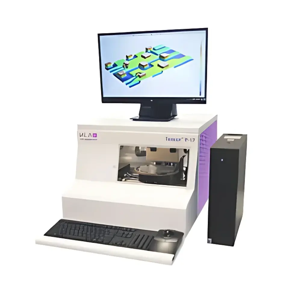
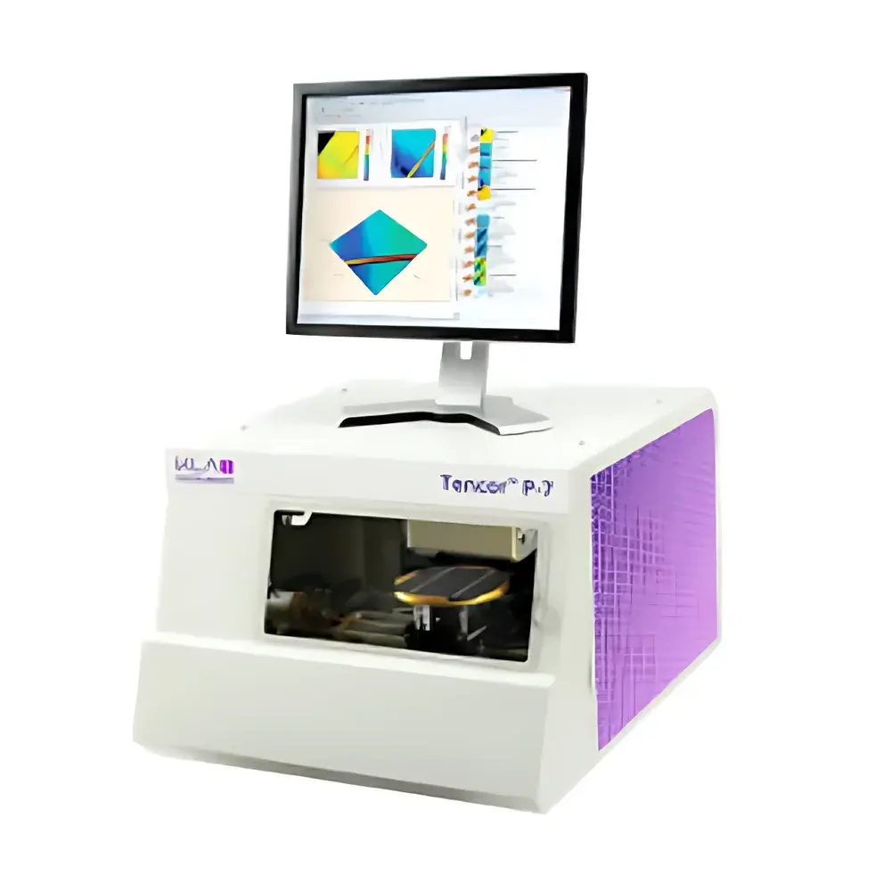
KLA Tencor P-7 Stylus Profilometer
| Brand | KLA |
|---|---|
| Origin | Malaysia |
| Manufacturer Type | Authorized Distributor |
| Origin Category | Imported |
| Model | P-7 |
| Measurement Principle | Contact Stylus Profilometry |
| Vertical Measurement Range | 1 nm to 1000 µm |
| Vertical Resolution | Sub-nanometer (typical) |
| Lateral Resolution | Determined by stylus tip radius (0.1–50 µm selectable) |
| Stylus Tip Radius | 0.7 µm (standard), down to 100 nm optional |
| Normal Force Range | 0.03–50 mg (force-controlled feedback) |
| Scan Length | Up to 150 mm (single-pass, no stitching required) |
| Wafer/Specimen Max Size | 150 mm diameter |
| Step Height Repeatability | < 0.2% of measured height (1σ) |
| Surface Flatness Calibration | Arc correction algorithm integrated |
| Imaging System | 5 MP color CCD with motorized zoom and focus |
| Software Platform | Apex™ v6.x with ISO/ASME-compliant analysis modules |
| Compliance | SEMI E4, E5, E30, E37 |
Overview
The KLA Tencor P-7 Stylus Profilometer is a high-precision, benchtop surface metrology instrument engineered for quantitative 2D and 3D topographic characterization in semiconductor process development, advanced packaging, MEMS fabrication, and thin-film R&D environments. It operates on the principle of contact stylus profilometry—where a diamond-tipped probe physically traces the sample surface under precisely regulated normal force, converting vertical displacement into high-fidelity analog voltage signals digitized at ≥16-bit resolution. Unlike optical methods, this technique delivers traceable, absolute height measurements independent of material optical properties, making it indispensable for measuring photoresist profiles, etch depths, CMP step heights, thin-film stress-induced wafer bow, and microstructured surfaces where transparency, reflectivity, or scattering limit interferometric or confocal approaches.
Key Features
- Single-pass 150 mm linear scan capability—eliminates stitching artifacts and ensures metrological continuity across full-diameter wafers and large-area substrates.
- Dynamic force control system maintaining constant normal load (0.03–50 mg) throughout measurement, enabling stable profiling of soft polymers (e.g., photoresists), fragile low-k dielectrics, and compliant organic layers without plastic deformation.
- Integrated arc correction algorithm compensates for vertical error induced by finite-radius stylus motion during lateral scanning—critical for accurate sidewall angle and step height fidelity.
- 5-megapixel motorized color imaging system with real-time overlay of scan path and feature coordinates, supporting precise region-of-interest targeting and post-scan defect localization.
- Modular stylus library with tip radii from 100 nm to 50 µm and included angles from 20° to 100°—enabling optimization for high-aspect-ratio trench profiling, nanoscale roughness, or macro-scale warpage.
- SECS/GEM and HSMS-compliant interface (SEMI E4/E5/E30/E37 certified) for integration into automated fab environments, including recipe-driven SPC data export, alarm forwarding, and remote diagnostics.
Sample Compatibility & Compliance
The P-7 accommodates specimens up to 150 mm in diameter using a vacuum chuck with precision locating pins. Its universal stage supports both flat and warped substrates via three-point kinematic mounting—essential for accurate stress-induced curvature quantification. Optional stages include solar-cell-specific carriers and 200 mm upgrade kits. All measurements adhere to ISO 25178 (surface texture), ISO 4287 (profile roughness), and ASME B46.1 standards when executed with Apex software. For regulated industries, optional Apex Enterprise licenses enable 21 CFR Part 11 compliance—including electronic signatures, audit trails, user access controls, and secure data archiving—fully aligned with GLP and GMP documentation requirements.
Software & Data Management
Apex™ software serves as the analytical core, offering ISO-compliant roughness (Sa, Sq, Sz), waviness (Wa, Wq), step height (Hstep), film stress (via Stoney equation implementation), and curvature radius calculations. Filtering options include Gaussian, spline, and robust polynomial detrending. Reports are exportable in PDF, CSV, and XML formats—with customizable pass/fail thresholds, annotated images, and multilingual support (11 languages). Offline Analysis software replicates full acquisition and analysis functionality on standard Windows workstations, decoupling method development from tool utilization. Graphical pattern recognition enables automated wafer alignment using pre-trained fiducials, reducing operator dependency and enhancing inter-tool reproducibility.
Applications
- Step Height Metrology: Quantification of deposited or removed layer thicknesses (e.g., SiO2, SiN, photoresist) following lithography, etch, deposition, or CMP—spanning 1 nm to 1000 µm with sub-angstrom repeatability.
- Surface Texture Analysis: Separation of roughness (Ra, Rq) and waviness (Wa, Wq) components per ISO 16610, supporting qualification of polishing processes and mold replication fidelity.
- Warpage & Shape Metrology: Full-diameter 2D bow mapping and 3D shape reconstruction—used to monitor thermal mismatch stress in heteroepitaxial stacks, MEMS package warpage, and lens curvature validation.
- Film Stress Calculation: Derivation of biaxial stress from surface topography changes before/after deposition, employing the modified Stoney equation with substrate modulus and Poisson’s ratio inputs.
- Defect Topography: KLARF-file-driven defect re-inspection with coordinate-based navigation, enabling depth profiling of scratches, particles, and delamination features in 2D cross-section or 3D volumetric view.
FAQ
What is the minimum measurable step height and its typical uncertainty?
The P-7 achieves sub-nanometer vertical resolution under optimized conditions; the practical lower limit for repeatable step height measurement is ~1 nm, with relative uncertainty ≤0.2% (1σ) for steps >10 nm.
Can the P-7 measure high-aspect-ratio structures such as deep trenches or vias?
Yes—using optional stylus tips with 20° included angle and 100 nm radius, the system resolves features with aspect ratios up to 10:1, provided sidewalls are accessible to physical probe contact.
Is NIST-traceable calibration supported?
Yes—VLSI Standards traceable step height reference artifacts (8 nm to 250 µm) are available and integrated into Apex calibration workflows, satisfying ISO/IEC 17025 laboratory accreditation requirements.
Does the system support automated batch measurement across multiple wafers?
With SECS/GEM connectivity and graphical pattern recognition, the P-7 executes unattended multi-wafer sequences—including auto-alignment, programmed scan grids, and SPC data streaming to host MES/SPC systems.
How is vibration isolation addressed in the P-7 platform?
KLA offers three isolation solutions: GraniteIsolator™ (passive granite/silicone), Onyx™ (pneumatic tabletop), and TMC 63-500 (freestanding pneumatic steel-frame)—all rated for <1 Hz resonance suppression and compatible with cleanroom Class 1000+ environments.