KMPR 1000 Series Negative Photoresist by MicroChem
| Brand | MicroChem |
|---|---|
| Origin | USA |
| Manufacturer Type | Authorized Distributor |
| Product Category | Imported Semiconductor Photoresist |
| Model | KMPR 1000 Series |
| Pricing | Available Upon Request |
| Developer Compatibility | PGMEA or TMAH aqueous solutions |
| Film Thickness Range | 2–75 µm (single spin-coat up to 100 µm) |
| Aspect Ratio | >5:1 |
| Adhesion | Enhanced metal adhesion |
| Stability | High electroplating bath compatibility |
| Cracking Resistance | Reduced thermal cracking tendency |
| Application Modes | Temporary or permanent patterning |
| Storage Temperature | –10 °C |
Overview
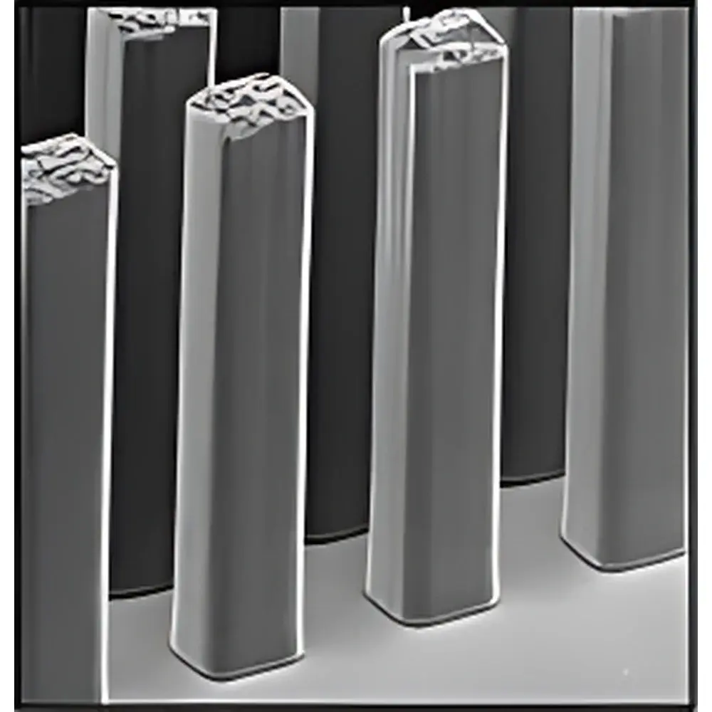
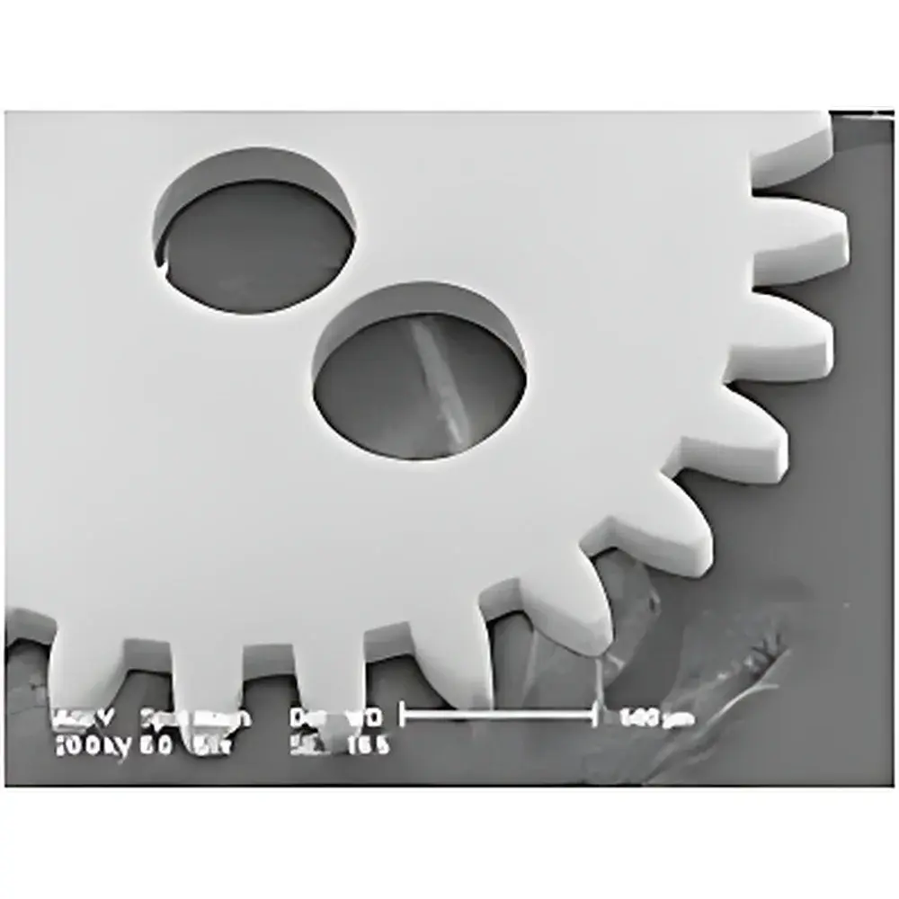
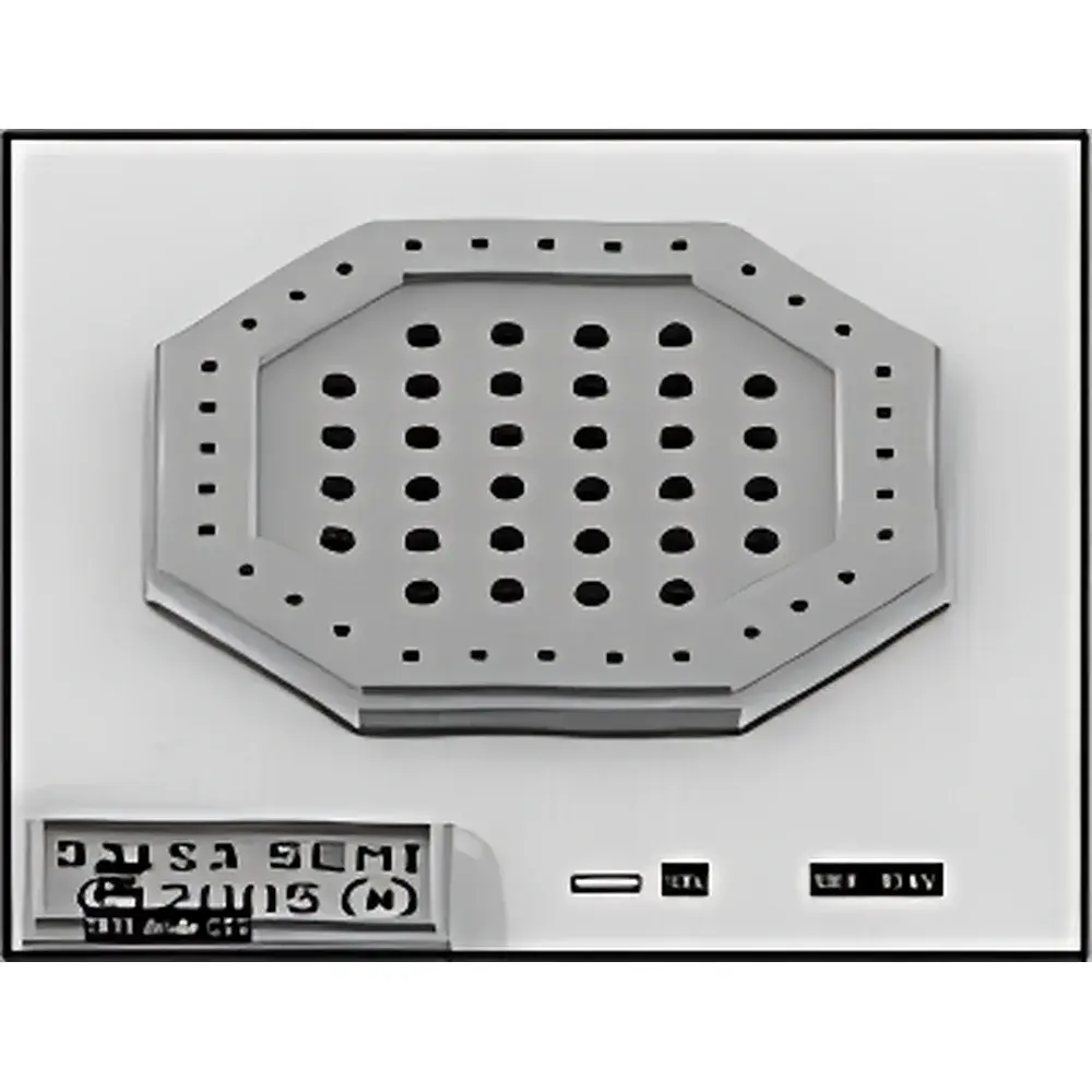
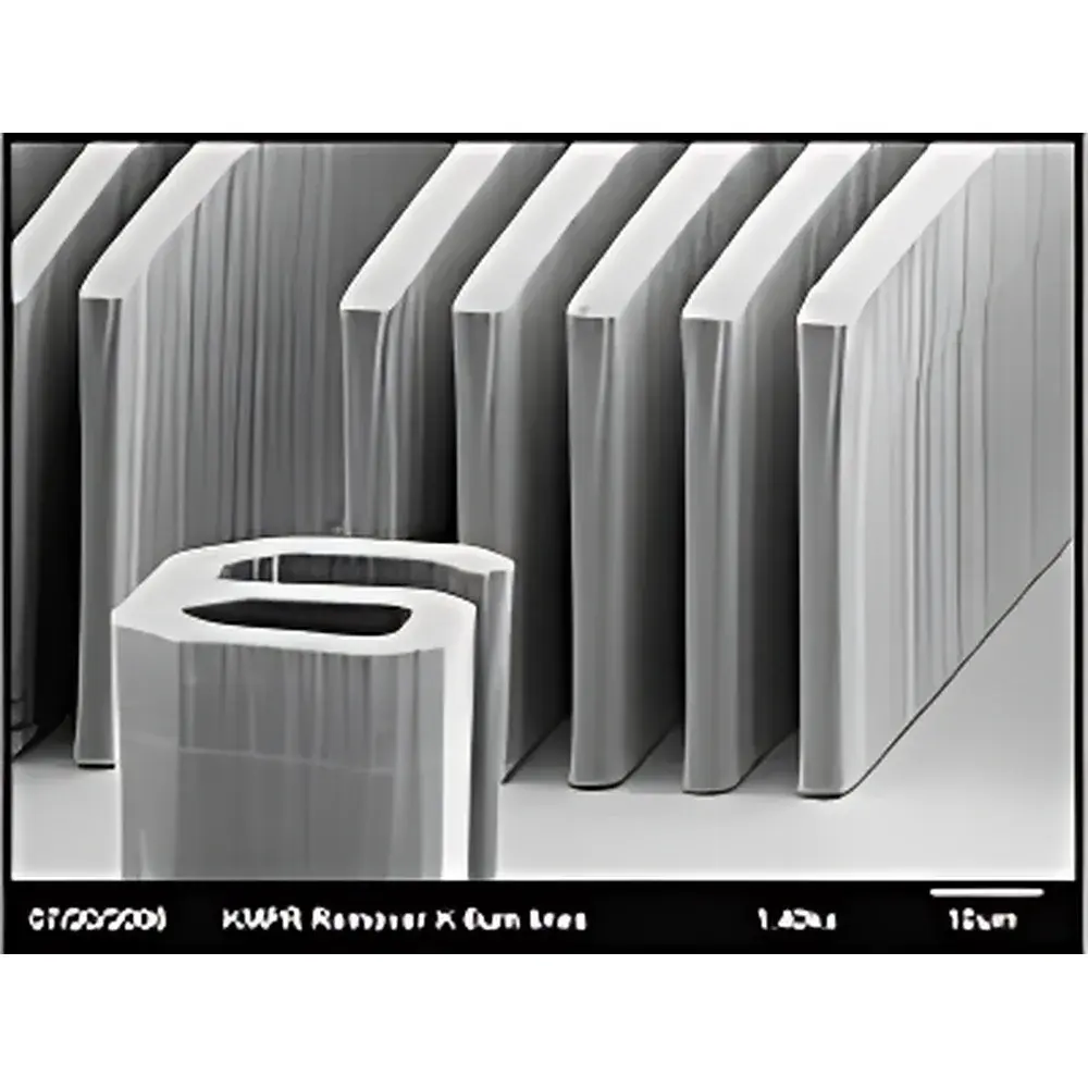
The KMPR 1000 Series is a high-performance, negative-tone photoresist engineered specifically for demanding microfabrication processes in semiconductor, MEMS, and bio-MEMS applications. Unlike conventional epoxy-based resists such as SU-8, KMPR utilizes a chemically amplified, low-crosslink-density formulation that enables superior process flexibility—particularly in lift-off, electroplating mold fabrication, and deep reactive ion etching (DRIE) hard mask applications. Its photoreaction mechanism relies on UV-induced acid-catalyzed crosslinking of poly(methyl methacrylate)-based polymers, resulting in high-resolution, vertically profiled features with aspect ratios exceeding 5:1. The resist is formulated for compatibility with standard semiconductor cleanroom infrastructure—including spin coaters, contact aligners, and UV exposure tools operating at i-line (365 nm) or broadband wavelengths. Its reduced crosslink density prior to post-exposure bake (PEB) and hard bake significantly improves removability compared to SU-8, facilitating both temporary patterning and permanent structural integration without residue or substrate damage.
Key Features
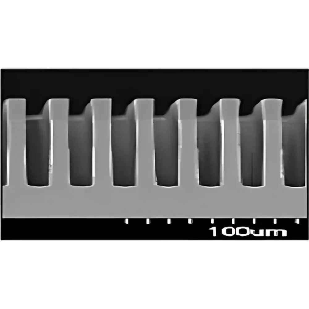
- Engineered for high-aspect-ratio patterning: Supports stable film formation from 2 µm to 75 µm via standard spin coating; single-layer deposition achievable up to 100 µm under optimized conditions.
- Vertical sidewall profile control: Delivers consistent, near-perpendicular feature walls essential for DRIE mask fidelity and electroplating mold integrity.
- Reduced thermal stress cracking: Lower crosslink density minimizes internal stress accumulation during thermal processing, improving film cohesion across large-area substrates and temperature-cycled processes.
- Enhanced adhesion to metallic layers: Demonstrates proven compatibility with Ni, Cu, Au, and Co electroplating baths—critical for LIGA-derived MEMS and RF/microwave component fabrication.
- Flexible developer compatibility: Fully processable using industry-standard aqueous developers including tetramethylammonium hydroxide (TMAH) and propylene glycol monomethyl ether acetate (PGMEA), enabling integration into existing lithography workflows without solvent requalification.
- Dual-mode application support: Suitable for both temporary masking (e.g., sacrificial etch masks) and permanent structural roles (e.g., microfluidic channel walls, RF shielding structures).
Sample Compatibility & Compliance
KMPR 1000 Series exhibits broad substrate compatibility—including silicon, SiO₂, SiNₓ, glass, quartz, and various metal films (Ti, Cr, Au, Ni). It conforms to standard semiconductor manufacturing cleanliness requirements (Class 100/ISO 5 cleanroom handling) and contains no halogenated solvents or heavy metals. While not certified under ISO 9001 or IATF 16949 directly (as a consumable material), its production adheres to MicroChem’s FDA-registered facility quality system, supporting GLP-compliant R&D documentation and traceability per batch lot number. Process validation data aligns with common industry benchmarks defined in SEMI Standard G40 (Photoresist Specifications) and ASTM F2219 (Standard Practice for Evaluating Photoresist Performance).
Software & Data Management
As a photoresist material—not an instrument—KMPR 1000 Series does not incorporate embedded software or digital interfaces. However, its process parameters are fully integrable into factory automation systems via standard recipe management protocols (SEMI E30/E40). Recommended process settings—including spin speed vs. final thickness correlation, soft-bake ramp profiles, UV dose calibration curves (mJ/cm²), and PEB time/temperature matrices—are documented in MicroChem’s Technical Data Sheets (TDS) and Process Integration Guides. These documents support electronic archiving, revision-controlled SOP development, and audit readiness for ISO/IEC 17025 or FDA 21 CFR Part 11–aligned quality systems when used in regulated environments.
Applications
- DRIE hard masks for silicon through-wafer vias (TSVs) and high-aspect-ratio trenches in power devices and image sensors.
- Electroplating molds for Ni and Cu microstructures in MEMS accelerometers, gyroscopes, and RF inductors.
- Bio-MEMS fabrication: microfluidic channel definition, cell-culture scaffolds, and biosensor electrode isolation layers.
- Temporary lift-off patterning for noble metal metallization in optoelectronic interconnects and plasmonic devices.
- Thick-film packaging layers for wafer-level chip-scale packaging (WLCSP) and fan-out wafer-level packaging (FOWLP).
FAQ
What developer solutions are compatible with KMPR 1000 Series?
KMPR is fully compatible with both aqueous TMAH (0.26 N) and organic PGMEA-based developers—no proprietary chemistry required.
Can KMPR be used as a permanent structural layer?
Yes. When fully cured via hard bake (>150 °C), KMPR achieves thermal stability up to 200 °C and mechanical robustness suitable for permanent device encapsulation or micro-mechanical elements.
How should KMPR be stored to maintain shelf life?
Store unopened bottles at –10 °C in the dark; avoid freeze-thaw cycling. Once thawed, use within 6 months under refrigerated (2–8 °C), nitrogen-purged conditions.
Is KMPR compatible with deep-UV (248 nm) or EUV lithography?
No. KMPR is optimized for i-line (365 nm) and broadband UV exposure; it is not formulated for DUV or EUV transparency or sensitivity.
Does KMPR require an adhesion promoter?
While optional, OmniCoat or similar HMDS-based primers are recommended for non-silicon substrates (e.g., metal or polymer) to ensure uniform wetting and edge bead removal.


