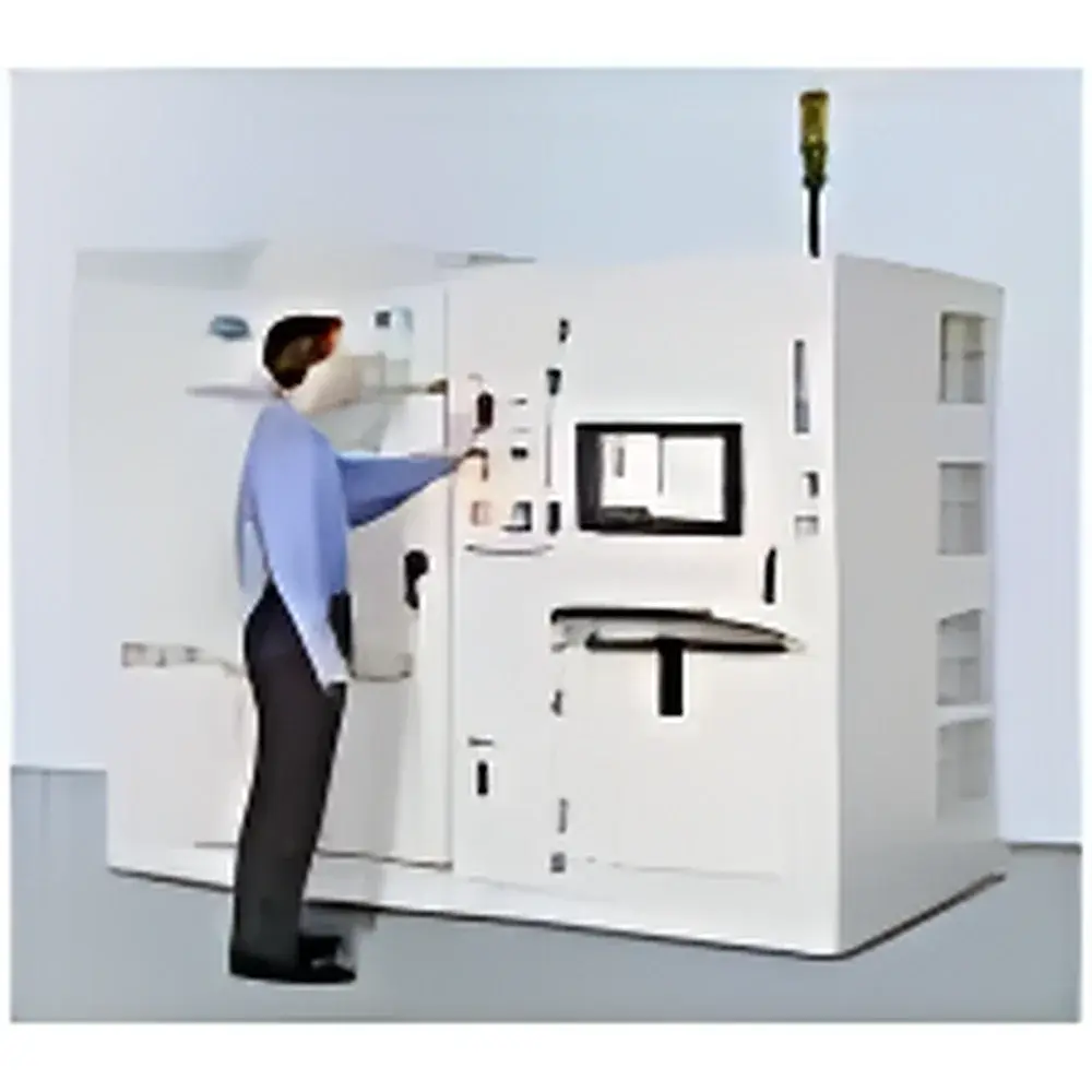
MCC LC-2 Advanced Burn-in Test System with Individual Chip Temperature Control
| Brand | MCC |
|---|---|
| Origin | USA |
| Manufacturer Type | Authorized Distributor |
| Origin Category | Imported |
| Model | LC-2 |
| Pricing | Upon Request |
| Board Dimensions | 317 mm × 609 mm (12.5″ × 24″) |
| Max Boards per System | 64 |
| Power per Board | Up to 400 W |
| Current per Board | Up to 240 A |
| I/O Channels | 128 independent |
| Vector Depth | Up to 4 M (upgradable) |
| Clock Resolution | 10 ns |
| Maximum Clock Frequency | 200 MHz |
| Max Device Power per Socket | 20 W |
| Concurrent Device Capacity | 1,536 devices |
| Thermal Control | Individual Chip Temperature Control (ICTC) via Pneumatic Cooling Valves and Heatsink-Based Resistive Heating |
Overview
The MCC LC-2 Advanced Burn-in Test System is a high-density, thermally intelligent platform engineered for reliability validation of integrated circuits across logic, memory, and power semiconductor applications. Built upon MCC’s proprietary Individual Chip Temperature Control (ICTC) architecture—first introduced in 1972—the LC-2 implements real-time, per-device thermal regulation using a dual-mode thermal actuation system: precision pneumatic air valves for rapid cooling and heatsink-integrated resistive heaters for stable, localized warming. Unlike conventional batch-heated burn-in ovens, the LC-2 applies calibrated thermal stress directly at the die level while maintaining strict voltage and current compliance per DUT. This enables accelerated life testing under conditions that replicate actual field operating temperatures—critical for identifying infant mortality failures in ASICs, DRAM, NAND flash, and high-power GaN/SiC devices. The system supports JEDEC JESD22-A108 and MIL-STD-883H Method 1005-compliant burn-in profiles, and its modular design integrates seamlessly into Class 1000 cleanroom environments.
Key Features
- Individual Chip Temperature Control (ICTC): Each device socket features independent thermal regulation via closed-loop feedback from on-board thermistors, enabling ±0.5 °C temperature stability across all 1,536 test sites.
- High-Power Density Architecture: Supports up to 400 W per 317 mm × 609 mm burn-in board, with per-socket limits of 20 W—optimized for modern high-current logic and power management ICs.
- Advanced Pattern Generation: 128-channel parallel I/O interface with 10 ns clock resolution and 200 MHz maximum frequency; vector depth scalable to 4 million patterns for complex functional stress sequences.
- Real-Time Power & Thermal Telemetry: Continuous monitoring of instantaneous voltage, current, junction temperature, and power dissipation per DUT—data logged at 1 Hz with timestamped audit trail.
- Modular Board Support: Accepts standard 12.5″ × 24″ (317 × 609 mm) burn-in boards; accommodates up to 64 boards per chassis for throughput scalability without compromising thermal uniformity.
- Compliance-Ready Firmware: Includes configurable logging, user-access controls, and electronic signature support aligned with FDA 21 CFR Part 11 and ISO/IEC 17025 documentation requirements.
Sample Compatibility & Compliance
The LC-2 supports industry-standard socket types including SOIC, QFP, BGA (up to 15×15 mm), LGA, and custom leadless packages—compatible with both ceramic and organic substrate ICs. It meets ASTM F1712-22 (Standard Guide for Burn-in Testing of Microelectronic Devices), adheres to JEDEC JEP122G failure mechanism models, and provides traceable calibration records per ISO/IEC 17025. All thermal control subsystems are validated against NIST-traceable references, and the system’s firmware includes GLP/GMP audit trail functionality for regulated semiconductor manufacturing facilities.
Software & Data Management
MCC BurnSuite™ v5.3 software provides full system orchestration—including test program loading, thermal profile definition, real-time dashboard visualization, and automated pass/fail classification. Raw telemetry data (temperature, VDD, IDD, thermal resistance) is exported in CSV and HDF5 formats for integration with enterprise MES platforms such as Siemens Opcenter or Applied Materials EnduraLink. The software supports role-based access control, electronic signatures, and secure data encryption (AES-256) compliant with ISO 27001 information security standards.
Applications
- Accelerated reliability screening of automotive-grade MCUs and ADAS SoCs under AEC-Q100 Grade 0–2 temperature profiles.
- Post-package qualification of high-bandwidth memory (HBM3, GDDR6X) under dynamic thermal load cycling.
- Wafer-level reliability validation for compound semiconductor RF power amplifiers (GaAs, GaN).
- Failure analysis correlation through synchronized thermal imaging and electrical parametric capture during burn-in.
- Qualification of AI accelerator ASICs requiring simultaneous high-voltage (1.8–3.3 V) and high-current (>5 A) stress conditions.
FAQ
What thermal accuracy does the ICTC system achieve per device?
±0.5 °C at steady state, verified using calibrated micro-thermocouples mounted adjacent to each socket.
Can the LC-2 be integrated into an existing factory automation system?
Yes—equipped with SECS/GEM protocol support, Modbus TCP, and RESTful API endpoints for bidirectional communication with host MES/SCADA systems.
Is firmware validation documentation available for regulated industries?
MCC provides IQ/OQ/PQ protocols, calibration certificates, and 21 CFR Part 11 compliance reports upon request.
What is the maximum allowable ambient temperature for continuous operation?
40 °C at 60% relative humidity, per UL 61010-1 and IEC 61000-6-4 EMC specifications.
How is electrical isolation maintained between high-power and low-voltage signal domains?
Galvanic isolation is implemented via optocoupled I/O buffers and segregated PCB layer stacks, meeting IPC-2221B creepage/clearance requirements for 300 V working voltage.


