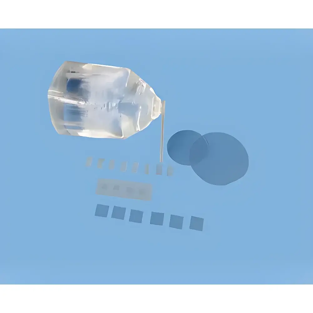
MgAl2O4 Spinel Single-Crystal Substrates
| Brand | 合肥科晶 |
|---|---|
| Origin | Anhui, China |
| Manufacturer Type | Authorized Distributor |
| Origin Category | Domestically Manufactured |
| Model | MgAl2O4 |
| Pricing | Upon Request |
| Crystal Structure | Cubic, Lattice Constant a = 8.085 Å |
| Growth Method | Czochralski (CZ) |
| Melting Point | 2130 °C |
| Density | 3.64 g/cm³ |
| Mohs Hardness | 8 |
| Thermal Expansion Coefficient | 7.45 × 10⁻⁶ /°C |
| Acoustic Velocity | 6500 m/s |
| [100] Shear Wave Propagation Loss (9 GHz) | 6.5 dB/µs |
| Color & Appearance | White, Transparent |
| Standard Orientations | <100>, <110>, <111> |
| Orientation Tolerance | ±0.5° |
| Standard Dimensions | 2" dia × 0.5 mm, 10 × 10 × 0.5 mm, 10 × 5 × 0.5 mm |
| Polishing | Single-side or double-side polished |
| Surface Roughness (Ra) | <5 Å |
| Packaging | Class 1000 cleanroom environment |
Overview
MgAl2O4 spinel single-crystal substrates are high-performance dielectric crystalline wafers engineered for demanding applications in surface acoustic wave (SAW) devices, bulk acoustic wave (BAW) resonators, microwave dielectric filters, and epitaxial growth of wide-bandgap semiconductors—particularly III–V nitrides such as GaN and AlN. As a cubic spinel-phase oxide with space group Fd3m, MgAl2O4 exhibits exceptional thermal stability, high mechanical hardness (Mohs 8), low dielectric loss, and excellent lattice matching with GaN (mismatch ~2.4% along ), making it a compelling alternative to sapphire (Al2O3) and SiC for heteroepitaxial device fabrication. Its high acoustic velocity (6500 m/s) and low shear-wave propagation loss (6.5 dB/µs at 9 GHz) support high-frequency SAW transducer design with improved insertion loss and temperature stability. Due to thermodynamic instability under stoichiometric melt conditions, high-quality bulk MgAl2O4 single crystals require precise control of oxygen partial pressure and thermal gradient during Czochralski growth—a capability rigorously validated across multiple production batches by the supplier.
Key Features
- Cubic spinel crystal structure with lattice constant a = 8.085 Å, enabling precise epitaxial registry for polar and non-polar III–N orientations
- Ultra-low surface roughness (Ra < 5 Å) achieved via chemical-mechanical polishing (CMP) on both single- and double-side polished variants
- Orientation tolerance tightly controlled to ±0.5° for , , and wafer planes—critical for reproducible thin-film nucleation and strain engineering
- Thermally robust architecture: melting point of 2130 °C and coefficient of thermal expansion (7.45 × 10⁻⁶/°C) compatible with high-temperature MOCVD and molecular beam epitaxy (MBE) processes
- Class 1000 cleanroom handling and Class 100 clean-bag or individual carrier packaging minimize particulate contamination and surface adsorption prior to deposition
Sample Compatibility & Compliance
These substrates are routinely employed in R&D and pilot-line fabrication environments compliant with ISO/IEC 17025-accredited metrology protocols. They meet material qualification requirements for semiconductor process development under JEDEC JESD22-A108 (temperature cycling) and MIL-STD-883 (microcircuit testing). While not certified to IEC 61215 or IEC 61730 (photovoltaic standards), their dimensional and surface specifications align with SEMI F48-0707 (specifications for compound semiconductor substrates) and ASTM F1531 (standard guide for characterization of single-crystal substrates). No hazardous substances are introduced during polishing or packaging; RoHS 3 (2015/863/EU) and REACH SVHC declarations are available upon request for full supply chain traceability.
Software & Data Management
As passive crystalline substrates, MgAl2O4 wafers do not incorporate embedded firmware or software interfaces. However, they are fully compatible with industry-standard thin-film metrology platforms—including ellipsometers (e.g., Woollam VASE), X-ray diffraction systems (Bruker D8 ADVANCE), and atomic force microscopes (Keysight 5500)—all of which support automated data logging, GLP-compliant audit trails, and export to CSV, XML, or HDF5 formats. Batch-specific certification reports include orientation verification (XRD θ–2θ scans), surface topography maps (AFM line profiles), and optical transmission spectra (200–2500 nm), archived digitally with timestamped QC sign-off per ISO 9001:2015 clause 8.5.2.
Applications
- Heteroepitaxial growth of GaN-based high-electron-mobility transistors (HEMTs) and light-emitting diodes (LEDs)
- High-frequency (>2 GHz) SAW and BAW resonator fabrication for 5G RF front-end modules
- Dielectric interlayer integration in multilayer ceramic capacitors (MLCCs) requiring low-loss, high-κ behavior
- Reference substrates for calibrating Raman spectroscopy intensity ratios in stress mapping of epitaxial layers
- Platform for fundamental studies of interfacial phonon coupling in oxide/III–N heterostructures
FAQ
What is the typical lead time for custom-oriented MgAl2O4 substrates?
Standard orientations (, , ) ship within 2–3 weeks from order confirmation. Custom orientations (e.g., off-axis ±0.2°) require crystallographic reorientation and additional XRD validation, extending lead time to 6–8 weeks.
Can these substrates be used directly in UHV MBE systems without pre-bake?
Yes—provided the substrates are transferred under inert atmosphere (N2 or Ar glovebox) and loaded into the MBE chamber using a load-lock system. A standard in-situ 500 °C, 30-minute anneal under O2 flux is recommended prior to GaN nucleation to desorb residual hydrocarbons and stabilize surface stoichiometry.
Is there batch-to-batch variation in lattice parameter or thermal expansion?
No. All production lots undergo post-growth high-resolution XRD (HR-XRD) with Si reference standard calibration. Lattice constant deviation is maintained within ±0.002 Å (0.025%) across consecutive batches, and thermal expansion coefficients are verified via dilatometry per ASTM E228.