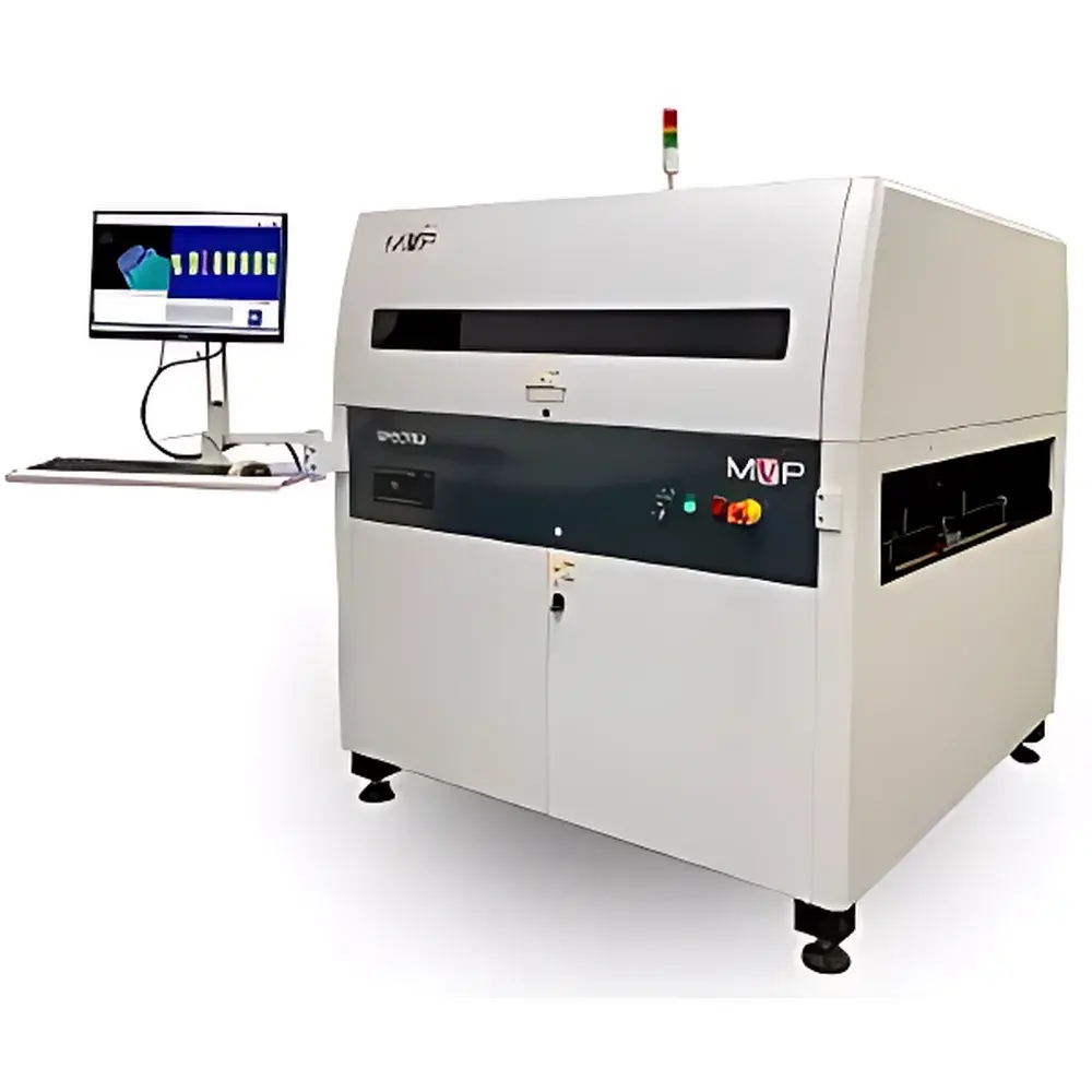
MVP Spectra Series II Large Format Automated Optical Inspection System
| Brand | MVP |
|---|---|
| Origin | USA |
| Manufacturer Type | Authorized Distributor |
| Origin Category | Imported |
| Model | Spectra Series II |
| Pricing | Upon Request |
Overview
The MVP Spectra Series II is a high-precision, large-format Automated Optical Inspection (AOI) system engineered for inline and offline quality assurance in advanced manufacturing environments. Utilizing synchronized 2D imaging, multi-spectral illumination (quad-color LED), and integrated 3D laser profiling, the system performs non-contact, high-speed surface and solder joint inspection based on geometric feature extraction, contrast analysis, and topographic deviation mapping. Its core architecture supports both reflective and diffuse surface evaluation across heterogeneous substrates—including laminated battery modules, rigid-flex backplanes, photovoltaic wafers, and large-area printed circuit boards—making it particularly suited for automotive electronics, electric vehicle (EV) powertrain assemblies, solar panel interconnect verification, and defense-grade display subsystems.
Key Features
- Standard inspection footprint of 35 × 35 inches (890 × 890 mm), expandable to 35 × 40 inches (890 × 1016 mm) via optional board indexing mechanism
- 3-axis flying stage with real-time motion synchronization to camera exposure and lighting triggers, enabling sub-millisecond dwell time per field-of-view
- Integrated dual-mode imaging: high-resolution 2D CMOS sensors (≥5 µm pixel resolution) coupled with Class 3R laser profilometry (±2.5 µm Z-axis repeatability)
- Quad-color programmable LED ring illuminator supporting spectral separation for enhanced contrast on matte, glossy, or metallized surfaces
- Optional paste volume measurement module compliant with IPC-7351B and IPC-A-610H solder paste deposition guidelines
- PIN-in-HOLE (PIH) inspection capability including lead coplanarity, insertion depth, and barrel fill assessment per IPC-J-STD-001G
- iPro and ePro software platforms featuring rule-based defect classification, statistical process control (SPC) dashboards, and automated report generation
Sample Compatibility & Compliance
The Spectra Series II accommodates rigid, flexible, and rigid-flex substrates up to 3 mm thickness and 25 kg maximum weight. It supports PCBs with standard FR-4, polyimide, ceramic, and metal-core laminates, as well as EV battery cell stacks with nickel-plated copper busbars and aluminum housing interfaces. The system meets CE marking requirements for electromagnetic compatibility (EN 61326-1) and functional safety (EN 61508 SIL2). Software audit trails comply with FDA 21 CFR Part 11 for electronic records and signatures when configured with user authentication, change logging, and data integrity controls. All inspection algorithms are traceable to NIST-traceable calibration standards and validated against IPC-A-610 Class 2 and Class 3 acceptance criteria.
Software & Data Management
iPro and ePro software suites provide a unified interface for recipe creation, defect review, and metrology reporting. Recipes support hierarchical parameter inheritance, allowing configuration reuse across product families while maintaining part-specific tolerances. Defect data is stored in an embedded SQLite database with optional ODBC export to enterprise MES or QMS platforms (e.g., Siemens Opcenter, Rockwell FactoryTalk). Real-time SPC charts monitor process capability indices (Cp/Cpk) for solder joint height, area coverage, and void percentage. Full system logs—including operator actions, image timestamps, hardware status, and calibration events—are retained for ≥18 months to satisfy GLP/GMP documentation requirements.
Applications
- EV battery module assembly: detection of tab weld anomalies, busbar misalignment, thermal pad coverage gaps, and insulation layer breaches
- Automotive ADAS backplane inspection: verification of blind via fill, microvia registration, and conformal coating uniformity on 12-layer HDI substrates
- Solar panel interconnect validation: identification of ribbon solder bridging, cracked cell fragments, and silver paste delamination at junction boxes
- Military/aerospace display assemblies: inspection of FPC-to-glass bonding integrity, EMI shield continuity, and touch sensor electrode continuity
- Large-format HMI panels: assessment of bezel alignment, lens clarity defects, and backlight uniformity across >24-inch active areas
FAQ
What is the minimum detectable defect size under standard illumination conditions?
The system achieves consistent detection of solder bridging ≥25 µm and component offset ≥30 µm on 0201–1206 packages, verified per IPC-AM-125G test patterns.
Does the Spectra Series II support AOI-to-SPI data correlation?
Yes—through standardized IPC-2581 export and native integration with leading SPI platforms, enabling closed-loop feedback for stencil design optimization.
Can the system be integrated into a factory-wide Industry 4.0 infrastructure?
It provides native OPC UA server functionality, MQTT publishing of key metrics, and RESTful API endpoints for job dispatch, result retrieval, and remote diagnostics.
Is training and technical support available globally?
MVP-certified application engineers deliver on-site commissioning, operator certification, and annual preventive maintenance programs aligned with ISO/IEC 17025 laboratory accreditation practices.